 Part of the Oxford Instruments Group
Expand
Collapse
Part of the Oxford Instruments Group
24 November 2020 | Andy Goodyear
When you plasma etch a wafer it is critically important for device performance to stop at the perfect etch depth. Using automatic endpoint technology during the etch provides realtime feedback and control, detecting precisely when to stop. In this blog, we reveal techniques to achieve the etch control you need through automatic endpoint technology.
Several techniques exist and it is vitally important to understand the strengths of each and how they fit with YOUR etch requirements to achieve what YOU need.
OES monitors the optical emissions from the plasma - the light intensity at various wavelengths. The spectrum of a plasma contains many emission peaks, each one corresponding to a particular atomic or molecular species within the plasma. We can detect when the etch transitions from one layer to another by detecting a change, e.g. a fall in Cr emissions when a Cr layer has been removed.
An OES endpoint kit consists of a spectrometer connected to a chamber viewport window via a fibre optic cable, see Fig.1. This feeds data to a PC which can be programmed to detect an endpoint signature, see Fig.2 for a typical endpoint trace.
As OES relies on plasma emissions, it typically requires fast etch rates and/or relatively large open (etched) areas, preferably full wafers, to provide enough etch by-products for the strongest endpoint signals.
If etching multilayer structures, OES has been shown to detect buried layers as thin as 10nm, providing accurate depth control.
OES also provides useful information about the chamber and process health, giving a fuller picture of the processing environment, and in some cases giving advance warning of potential problems. It is very useful when running a plasma cleaning process as it can detect when the materials on the sidewalls have been removed.
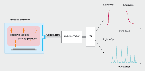
Fig 1. OES Endpoint setup
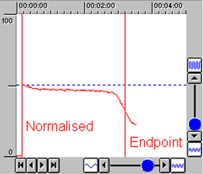
Fig 2. OES endpoint of photoresist removal
Laser interferometry monitors the wafer directly by focusing a small laser spot (~20-60μm diameter and 670, 905 or 980nm wavelength) onto its surface and measuring the reflected light intensity.
A special camera is mounted on top of the etch chamber (Fig.3), providing a TV image of the wafer surface and focusing a laser spot onto the wafer. The camera also collects the reflected laser light to provide a measure of the wafer reflectance. The spot can be positioned at a particular point on the wafer surface, via movement of the camera’s x-y table. The laser spot is usually placed on an open area of the wafer, ideally >100x100μm near the centre of the wafer.
Laser interferometry has the advantage that it can measure small samples (e.g. wafer pieces) and can measure etch depth within a transparent layer.
As manual positioning of the spot is required in each run, laser endpointing is not commonly used in a production environment, unless a larger test area (up to 1x1mm) is provided near the centre of the wafer.
In some applications, such as metal etching, there may be a simple change in reflectance as the layer is removed. If etching a transparent layer, the etch depth can be measured by counting ripples in the reflected intensity. These ripples come from interference effects within the layer as its thickness changes, see Fig.4 for example.
If the wafer has a multilayer structure then the reflectance trace can be more complex, typically requiring reflectance modelling and careful choice of endpoint algorithms to stop the etch at the correct depth.
As the laser is focussed on a single small spot then the endpoint trace will show layer interfaces very distinctly, especially under high contrast conditions, see the upper trace of Fig.3. If ‘etching to depth’ via ripple counting then accuracy is typically +/1% or less, assuming a sufficient number of ripples are present and the refractive index of the layer is well-characterised.
However, as with all endpoint techniques, absolute depth accuracy will also depend on etch rate, sampling/smoothing rates and across-wafer uniformity.
At Oxford Instruments we can provide a variety of OES and LI systems, ranging from cost-effective general-purpose kits to high sensitivity systems with sophisticated endpoint algorithms.
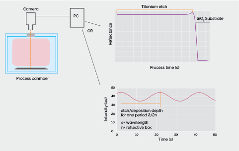
Fig 3. Laser endpoint setup
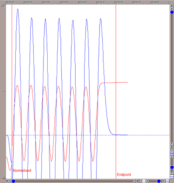
Fig 4. Laser endpoint trace showing removal
of a transparent layer on a Si wafer.
Table 1 below shows some typical criteria and table 2 shows a guide for applications. For more information please get in touch with us at plasma-experts@oxinst.com.
Table 1. Typical criteria for the endpoint techniques
| Property | OES | Laser |
| Sample Size | Large samples/wafers only | Any size sample |
| Endpoint detection area | Global/batch | Localized detection at spot |
| Endpoint type | Only layer transitions | Transitions or etch depth in-layer |
| Patter requirements | Any size/shape/location, if total exposed area is sufficient | >100x100μm needed close to the centre of the wafer for manual spot positioning |
| Operation | Fully automated | Manual spot positioning, unless a much larger test area is provided |
Table 2. Typical applications for the endpoint techniques.
| Application | OES | Laser |
| Chamber cleaning | ✓ | x |
| In-layer depth targeting | x | ✓ |
| Complex multilayers (e.g. metal/oxides, III-V) | ✓ | ✓ |
| Dieletric thin film removal | ✓ | ✓ |
| Metal thin film removal | ✓ | ✓ |
| Failure Analysis | Large samples only | ✓ |
| SOI Endpoint | ARDE effects | ARDE effects |
| Plasma analysis/chamber condition monitoring | ✓ | x |
Find out more about other endpoint techniques (such as large spot interferometry, in-situ ellipsometry, ion mass spectrometry, or process readbacks) in our second blog on endpoint techniques coming soon.
If you would like to learn more about endpoint solutions, take a look at our Automatic Endpoint Detectors.
Dr Andy Goodyear
Principal Applications Specialist


2020
2019

© Oxford Instruments 2026

