 Part of the Oxford Instruments Group
Expand
Collapse
Part of the Oxford Instruments Group
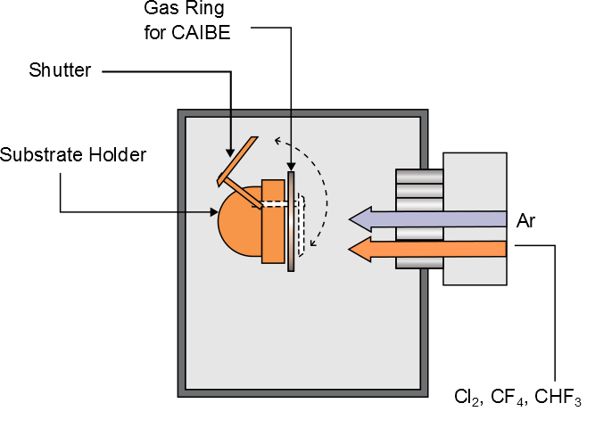
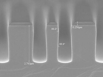
Ion Beam Etching (or Milling with inert gases) is achieved by directing a beam of charged particles (ions) at a substrate with a suitably patterned mask in a high vacuum chamber. It enables highly directional beams of ions – whose space-charge is neutralised by electrons from the neutraliser - to control the etched sidewall profile as well as radial uniformity optimisation and feature shaping during nanopatterning notably using the tilt angle to the beam with on-axis rotation for axisymmetry.
On the other hand, angled features can be created by the unique ability to tilt the sample (without rotation) altering the direction of impact of the ion beam. In both cases, the etch process can be assisted by chemistry (RIBE and CAIBE) using reactive gases to enhance both etch rates and selectivity to a mask.
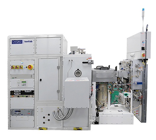
The Ionfab® system offers maximum flexibility coupled with excellent uniformity for fast process development and repeatable process results.
| Ionfab | |
| Ion Etching Source | 150mm or 300mm for up to 4" and 8" respectively |
| Etching Area | Up to 200mm diameter or 150mm square |
| Platen Speed | Up to 20rpm |
| Platen Tilt Angle | 0º to 75º between beam and normal to substrate surface |
| Platen Heat | Embedded heaters up to 300ºC with PID control |
| Platen Cooling | Fluid coolant 5ºC to 60ºC with He or Ar backside gas for substrate cooling (up to 50Torr) |
Ion beam etching can be applied in two ways: using inert ions for a physical etching or milling process or using RIBE/CAIBE with reactive ion species to increase differential material etch rates with a chemical/reactive component and enhance selectivities.
In Reactive Ion Beam Etching (RIBE) and Chemically Assisted Ion Beam Etching (CAIBE) modes, reactive species are added (CHF3, SF6, N2, O2, etc.) to the source (RIBE) or to the gas ring (CAIBE) to increase volatility of etch products and selectivity to the mask material.
Ionfab provides flexible hardware options including single substrate loadlock and cassette-to-cassette. Its multiple mode functionality enables high throughput with reduced footprint.

© Oxford Instruments 2026

