 Part of the Oxford Instruments Group
Expand
Collapse
Part of the Oxford Instruments Group
Welcome to the first issue of Semi Interface, representing a community of technology experts with interesting insights to share for increasing device performance through material interface engineering and optimisation, as well as other semiconductor industry challenges.
Our contributors share their vast experience, with one story demonstrating how interface optimisation history is repeating itself, plenty of discussion on the latest techniques for interface optimisation and material engineering, as well as insights on interface challenges of the near future.
Download Magazine
"You are touching upon the most important and complex topic in Semiconductor devices: all the device scientists and engineers will be interested in this topic. My heartiest congratulations to you."
Dr Aryasomayajula Subrahmanyam
Professor (Retd), Physics, IIT Madras, India
Dr-Eng. S.K. Murad, technology consultant and managing director at GaN Consultancy, discusses the crucial need for improving interface engineering in the world of advanced semiconductor devices. He delves into the importance of enhancing the quality of both surface and interface, as well as the optimization techniques that can be used to help make this possible.
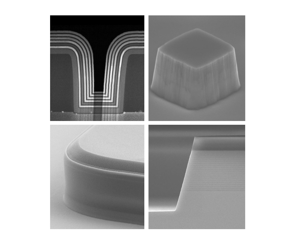
Frazer Anderson, chief technical officer at Oxford Instruments Plasma Technology, speaks about the increasing complexities of atomic-scale processing and measurement analysis. From atomic layer etching (ALE) to electron backscatter diffraction (EBSD), Frazer discusses ways in which increasingly popular compound semiconductor materials can be fabricated and analysed, using highly specialised processes and characterisation techniques.

“It is therefore crucial to be able to both fabricate and characterise these interfaces at the nanoscale in 3 dimensions.”
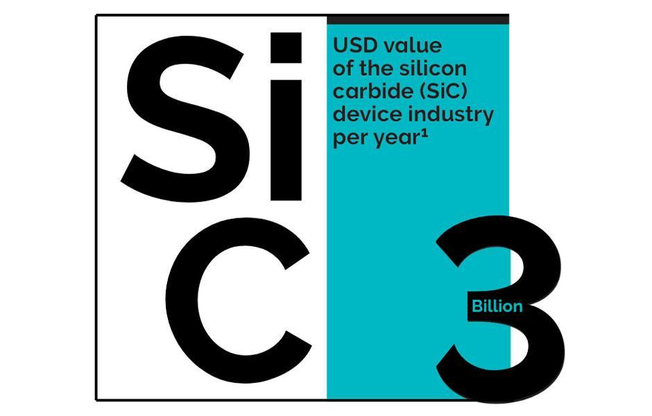
It’s that time of year again, and Oxford Instruments are delighted to be back at ICSCRM, one of the biggest global events for silicon carbide (SiC) device processing. We show some of the exciting projects that Oxford Instruments are supporting and promoting at the conference – multiple projects with Warwick University, including void-free superjunction trench fill and post-trench annealing to optimise base rounding, as well as promising process results with SK Siltron for Plasma Polish, our SiC substrate and epi layer dry etch technique to remove defects and subsurface damage.

“SK Siltron see the potential benefit of Plasma Polish to access and remove subsurface damage.”
Executive Director & CTO of PowerAmerica, Prof. Victor Veliadis, explores the SiC/SiO2 gate interface of SiC metal-oxide semiconductor field effect transistor (MOSFET) devices and how it’s quality still challenges device manufacturers today. Prof. Veliadis discusses the problems faced by this interface and what tools, such as Oxford Instrument’s atomic layer deposition (ALD) technology, can help to improve the SiC/SiO2 interface.

"ALE minimises surface damage and produces low defect interfaces and low roughness sidewalls for high mobility.”
In the 1st of a 2-part series about the SiC gate oxide, Prof. Peter Gammon from the School of Engineering at the University of Warwick and the founder of PGC consultancy, gives us a detailed insight into the background of SiC versus Si devices, the challenges that come with SiC MOSFETs and how nitrogen has come to the rescue.
Dr Dan Haspel, key account manager at Oxford Instruments Plasma Technology, highlights the essential need to combine multiple analytical microscopy techniques to get a more accurate and in-depth understanding of your devices. He touches on 3 complementary microscopy methods – electron backscattering diffraction (EBSD), Raman and contact resonance atomic force microscopy (CR-AFM) - that Plasma Technology use to characterise and assess the quality of the SiC surface, subsurface and deeper into the crystal structure.

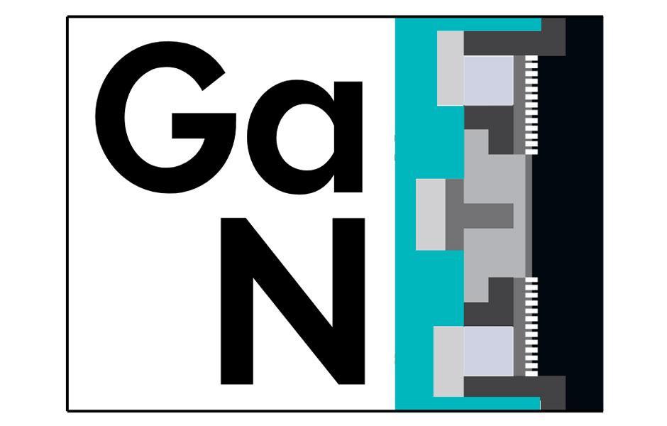
Dr Aileen O'Mahony, atomic scale processing product manager at Oxford Instruments Plasma Technology, shares her expertise on GaN devices. She discusses the critical 2-dimensional electron gas (2DEG) layer at the AlGaN/GaN interface and how the combination of conventional inductively coupled plasma (ICP) etch and atomic layer etch (ALE), can provide enhanced etch control.
Dr Zhong Ren, principal applications engineer at Oxford Instruments Plasma Technology and Dr Marta Kocun, product line manager at Oxford Instruments Asylum Research, discuss their work on through silicon vias (TSVs) for quantum computing. They share data from our post-Bosch TSV Plasma Polish interface optimization process, to achieve atomic layer deposition (ALD) ready smooth sidewalls, along with informative atomic force microscopy (AFM) results.

“Superconducting through silicon vias (TSVs) are key to realising scalable superconducting quantum computing (SQC) platforms, because they enable more qubits, denser integration, and longer coherence times.”
Prof. Paul Hurley, Head of the Nanoelectronic Materials and Devices Group at the Tyndall National Institute and a Research Professor in the Department of Chemistry at University College Cork, sat down with Dr Aileen O’Mahony to talk all things interfaces. He goes through the fascinating history of transistors and how the past and present can come together to help create the future of semiconductor devices.

“Breakthroughs come from when people from different backgrounds come together.”
Global Sales and Marketing Director for Oxford Instruments Plasma Technology, Bas Derksema spoke with Grant Baldwin, editor of Semi Interface and head of marketing for Oxford Instruments Plasma Technology, about the company’s expansion to high-volume manufacturing and what measures we are taking to ensure the highest quality equipment and processes are available to customers.
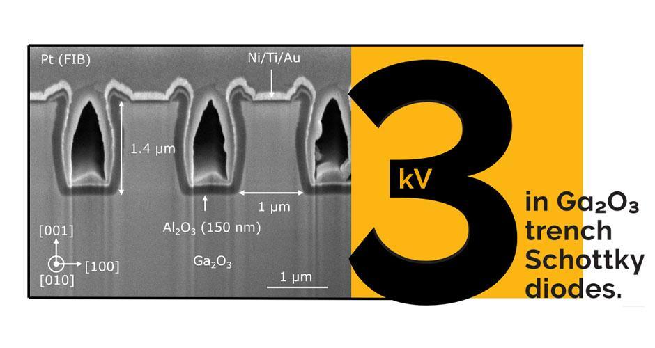
A team led by Prof. Martin Kuball at the University of Bristol discuss their work on (ultra)-wide bandgap materials as semiconductor materials, with a focus on Ga2O3. They share key insights about the impact of the orientation of trenches in devices, along with promising experimental breakdown voltage results.
Dr Julian Michaels, postdoctoral research assistant collaborating with Argonne National Laboratory and Oxford Instruments Plasma Technology, speaks about his work on biased-pulsed atomic layer etching (BP-ALE) for the controlled fabrication of 4H-SiC devices. He highlights the smoothing effect of BP-ALE, and how this modified fast ALE technique could be implemented for mainstream device production.

“As our world approaches the nanoscale, atomic scale processing will be ever more crucial; at the same time, processing duration must not grow excessively.”
As we have seen in issue 1 of Semi Interface, device performance is heavily influenced by the interface, and similar solutions that optimise the interface at an atomic level can be applied in quantum and GaN & SiC power, but also in many other markets like datacom, augmented reality and microLEDs. The theme of issue 2 will be optoelectronics and datacom, plus a few part 2 articles to some of our authors’ contributions from issue 1.
Do you have insights to share? We are particularly interested in gathering expert perspectives from device manufacturers, in addition to industry analysts and researchers. Join the Semi Interface community by downloading our magazine and get involved with your own article submission by clicking the link below.
Submit the Article
© Oxford Instruments 2026

