 Part of the Oxford Instruments Group
Expand
Collapse
Part of the Oxford Instruments Group
With systems designed for high volume manufacturing (HVM) or research and development we deliver the hardware and process solutions you need for your Lab or Fab. Our plasma processing technology offers a wide range of advanced capabilities for etching, deposition and material growth. With over 8,000 recipes in our library, we provide process development and support, customised to our customers' needs, enabling them to achieve the right cost of ownership with high wafer yield and fast, high-performance processing.
Plasma process is essential for manufacturing of advanced microelectronics. Our plasma processes provide the reliability to confidently achieve the desired device characteristics. Our versatile plasma etching and deposition tools deliver:

Dielectric metal plasma RIE etching

ICP Chemical Vapour Deposition
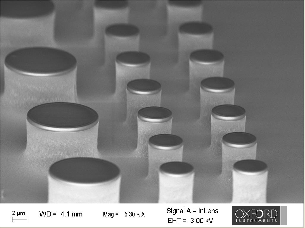
Ion beam etch and ion beam deposition offers film quality and etch control coupled with excellent uniformity. It is ideal for a wide range of applications such as MRAM, laser bar facets and thin film magnetic heads. Ion beam technology enables researchers and high volume manufacturers to produce dense, high quality films with smooth surfaces.
Ion Beam Etching electron
Many advanced devices require atomic scale precision during fabrication, to deliver the accuracy needed we provide the advanced processing techniques of atomic layer etching and deposition. This capability to manipulate and control matter precisely enables R&D and production of the next generation of semiconductor devices.
This technique is designed to allow the accurate removal of one atomic layer at a time; a level of control unachievable using conventional etching.
This technique offers precisely controlled deposition of films for advanced applications with a single atomic layer deposited per process cycle, it is self-limiting and gives conformal coating into high aspect ratio structures.

Atomic layer deposition of dielectrics & metals
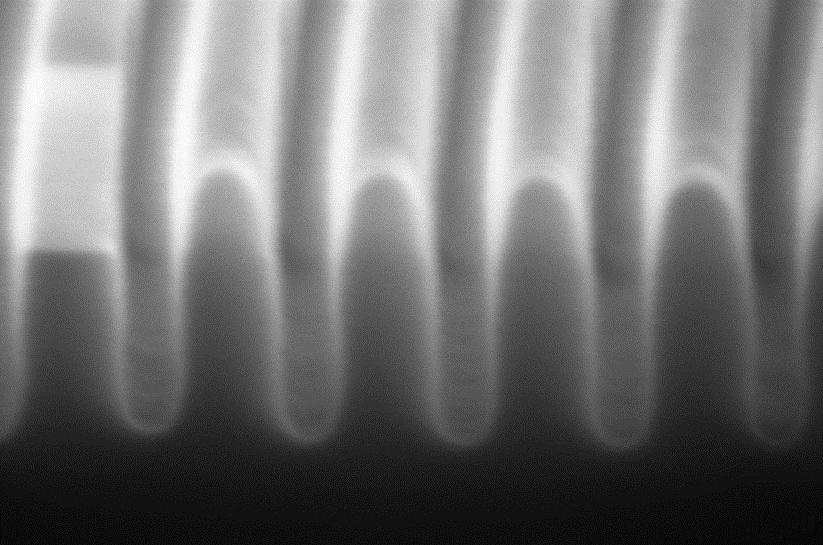
25nm wide Si trenches etched to 110nm depth by ALE
For questions about our plasma process technologies, or for more information on any of our technologies, please contact our experts at plasma-experts@oxinst.com. We'll be more than happy to help.

© Oxford Instruments 2026

