

Oxford Instruments enables ROHM’s in-house GaN manufacturing with…
Oxford Instruments, a leading provider of advanced plasma processing solutions…
 Part of the Oxford Instruments Group
Reactive ion etching (RIE) is a simple operation and an economical solution for general plasma etching. A single RF plasma source determines both ion density and energy. Our RIE modules deliver anisotropic dry etching for an extensive range of processes.
Multiple choices of etch processes:
RIE features:
A wide range of materials can be etched, including:
Plasma RIE-PE (reactive ion etching - plasma enhanced) combines two simple plasma generation techniques on one tool.
With RIE, more directional etching and faster rates are achieved as the surface the sample sits on has an accelerating voltage attracting ions from the plasma. Plasma has no accelerating voltage and more isotropic etching takes place.
The PlasmaPro 100 RIE modules deliver isotropic and anisotropic dry etching for an extensive range of processes. It is suitable for research and production customers, providing a controlled environment that improves process repeatability with load-lock and cassette-to-cassette options.
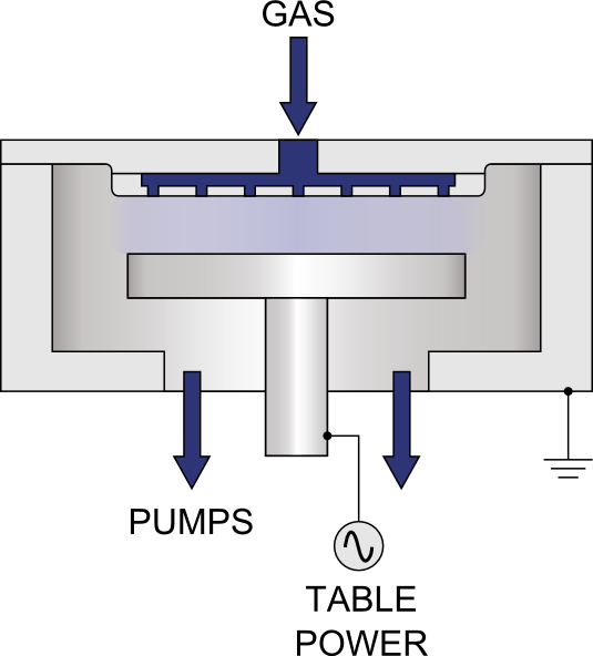
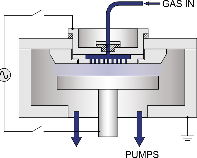
RIE is a predominantly physical etch process. A rich plasma is created just above the wafer and the ions are accelerated toward the surface to produce a powerful and highly anisotropic etch. Gas enters the top of the chamber where it is converted into a reactive plasma at low pressure by a wafer-level RF source. The ions either interact with the sample to form etch by-products, or remain as unreacted species. All the unreacted species and by-products are removed from the chamber by the vacuum pump to maintain a rich and active plasma to maintain high etch rates.
The PlasmaPro 100 RIE delivers reactive species to the substrate, with a uniform high conductance path through the chamber, allowing a high gas flow to be used while maintaining low pressure.
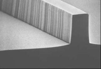
RIE of InP waveguide
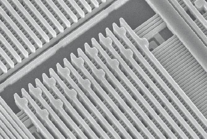
Dielectric metal etch - Courtesy of Atmel
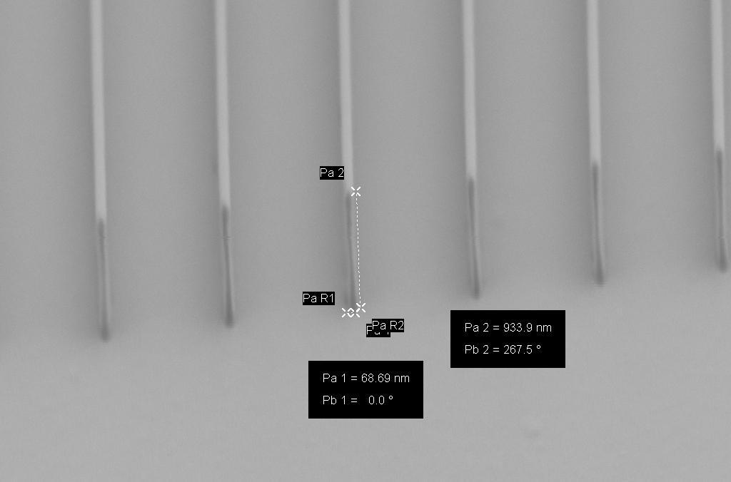
70 nm Fused Silica lines 933 nm deep Cr mask - Courtesy of Cornell Nanoscience facility
Cluster load lock options
*with MX600ss
Typical conditions
Advanced load lock options
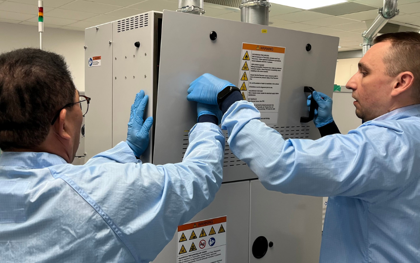
Oxford Instruments is committed to providing a comprehensive, flexible and reliable global customer support. We offer excellent quality service throughout the life of your system.
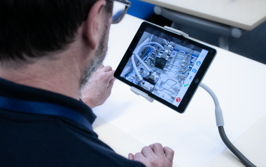
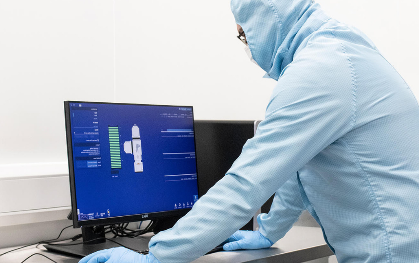
PTIQ is the latest intelligent software solution for PlasmaPro and Ionfab processing equipment.
At Oxford Instruments Plasma Technology, we offer a wide range of technical training courses designed to suit all skill levels and needs.

© Oxford Instruments 2026