 Part of the Oxford Instruments Group
Expand
Collapse
Part of the Oxford Instruments Group
Yield management is a key factor in semiconductor manufacturing. To improve yield, one key technique is the de-processing of a failed chip or wafer to find and analyse the failure point in order to eliminate it.
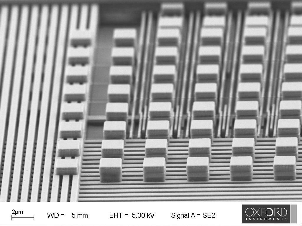
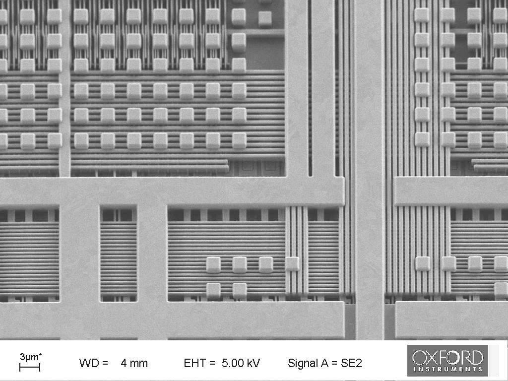
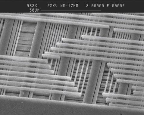
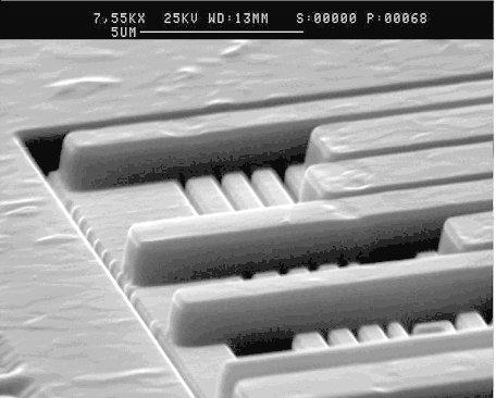
For analysis or defect identification to be performed the device must be suitably prepared, this becomes more challenging as device architectures become ever more 3-dimensional. Plasma assisted etch and deposition are used to ensure accurate, quickly achieved results.
Oxford Instruments’ flexible Failure Analysis (FA) tools allow a wide range of processes, able to process small die or packaged devices through to 300mm wafers. Well controlled processing means that there is no damage to the metal conducting tracks.

© Oxford Instruments 2026

