

Oxford Instruments enables ROHM’s in-house GaN manufacturing with…
Oxford Instruments, a leading provider of advanced plasma processing solutions…
 Part of the Oxford Instruments Group
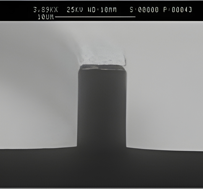
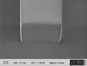
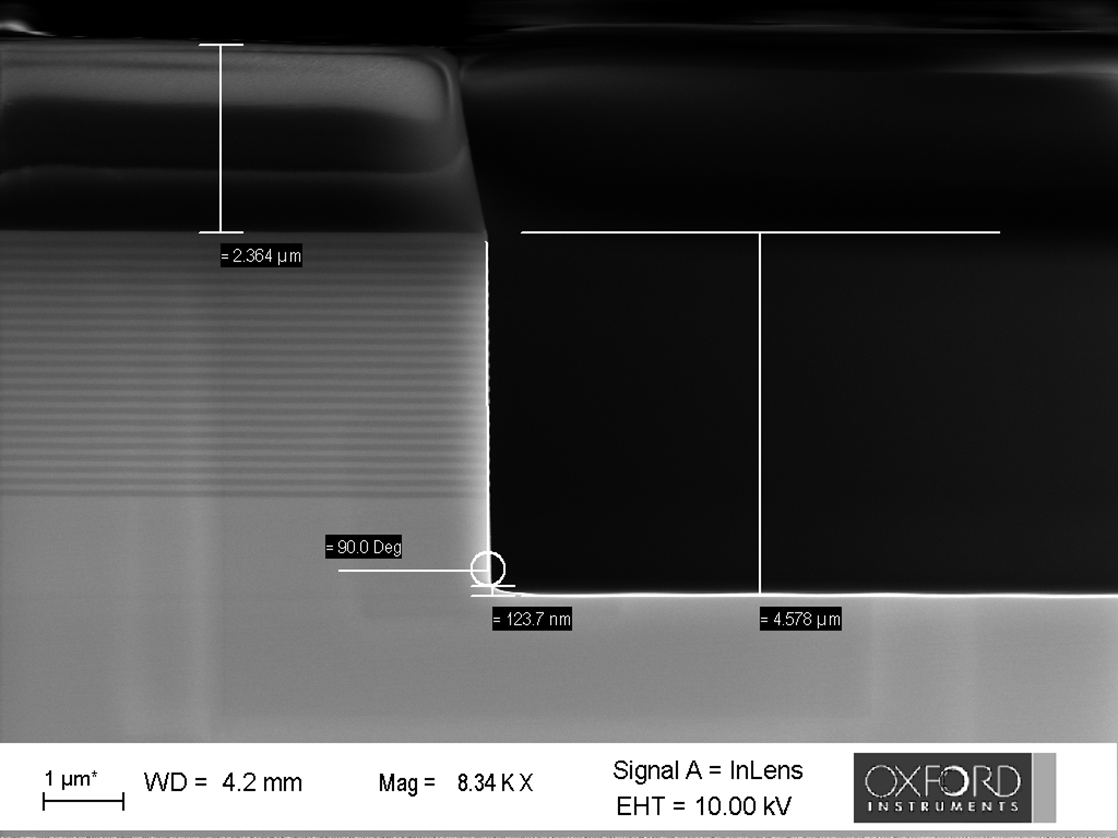
ICP etching of a InP showing smooth sidewalls and clean etched surface
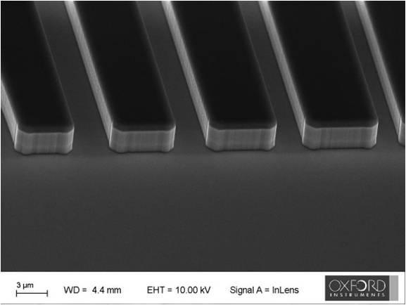
ICP etching of SiO2 waveguide using a Cr mask
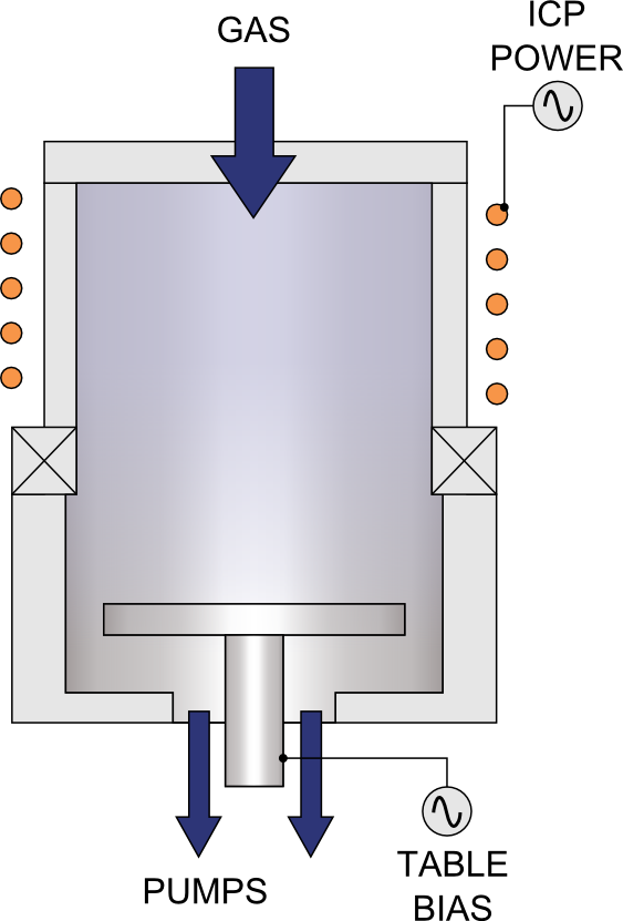
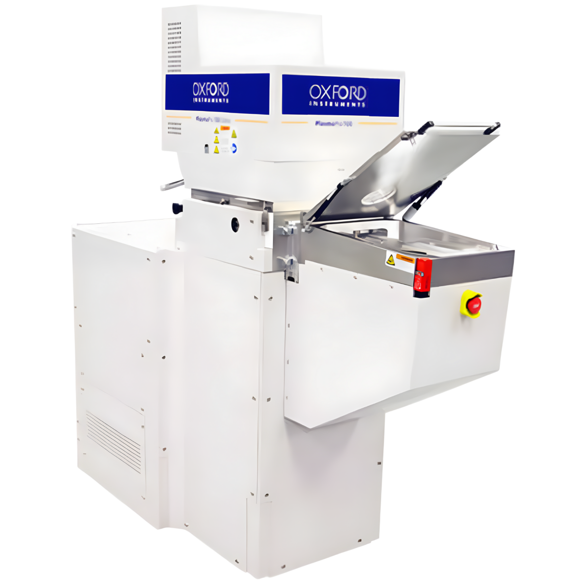
The PlasmaPro 100 Cobra ICP RIE system utilises a high-density inductively coupled plasma to achieve fast etch rates. The process modules offer excellent uniformity, high-throughput, high-precision and low-damage processes for wafer sizes up to 200 mm, supporting a number of markets including, GaAs & InP laser optoelectronics, microLEDs & metalenses, SiC & GaN power electronics/RF and MEMS & sensors.
*dependent on chiller option selected.

As VCSEL shipment volume increases, Oxford Instruments enables its customer to improve yield and drive manufacturing cost down.
Our systems are well proven, with over 90% uptime and processes that are guaranteed to ensure rapid startup during installation.
Vertical Cavity Surface Emitting Lasers (VCSEL) is a technology of choice for applications where compact size, high beam stability and low power consumption matters.
We applied our processing knowledge to enable device cost and performance and maximize production of good die per day.
VCSELs are used in Light Detection And Ranging (LiDAR), enabling autonomous vehicles to detect distances and movement. Other applications of VCSEL is in 3D sensing for facial, object and gesture recognition, and biometric payments.

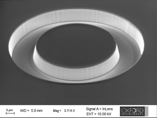
VCSEL mesa Top view
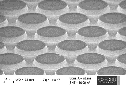
VCSEL mesa Top view
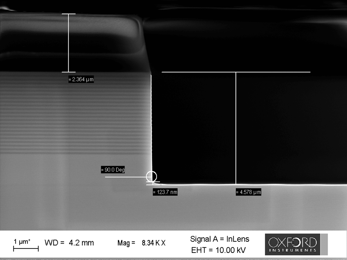
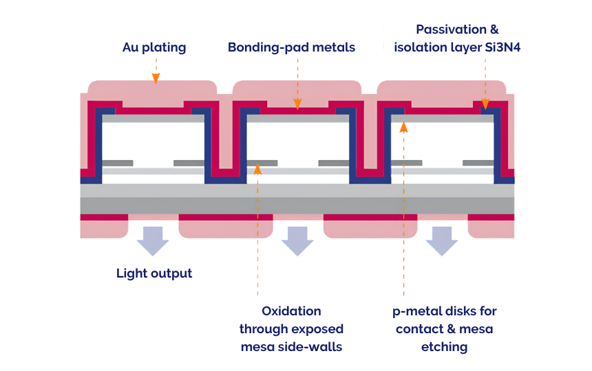
VCSEL mesa vertical cross section
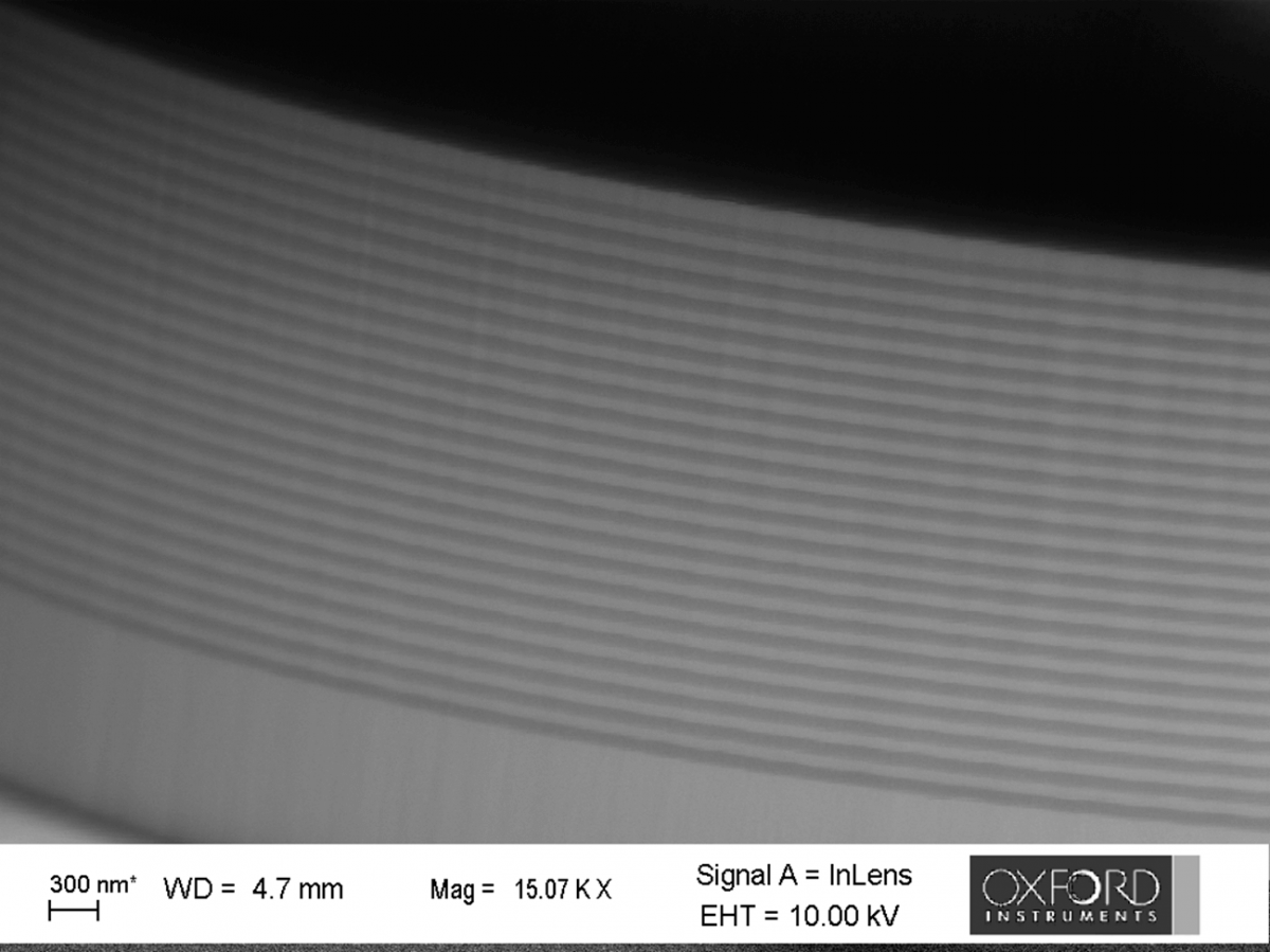
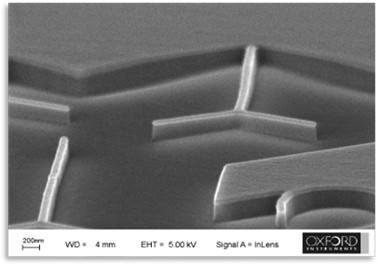
High surface quality
VCSEL is a technology of choice for applications where compact size, high beam stability and low power consumption matters.
We applied our processing knowledge to enable device cost and performance and maximise production of good die per day.
VCSELs are used in light detection and ranging (LiDAR), enabling autonomous vehicles to detect distances and movement. Other applications of VCSEL is in 3D sensing for facial, object and gesture recognition, and biometric payments.

LiDAR

Biometric payment

Face ID

Gesture recognition
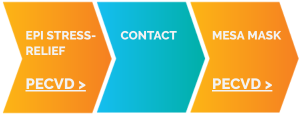
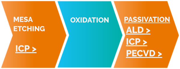

Simplified process flow. Orange processes show solutions covered by Oxford Instruments' technology. ICP Etching is covered by PlasmaPro 100 Cobra™ GaAs VCSEL.
Endpoint techniques enable a tighter distribution of etching depth to a target layer by allowing for run-run etch variations as well as variations in the incoming material target thicknesses.
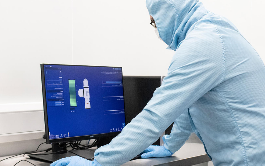
Our PTIQ system software has been designed to deliver an exceptional level of responsive system control, reliability and repeatability for Oxford Instruments customers. It will optimise system and process performance in the Lab or Fab, with different levels of software available to suit facility requirements.
We have introduced a unique patented approach to achieve low damage and high-quality SiC substrate polishing on our 200 mm production platform. Plasma polish has been proven to produce a damage-free surface and subsurface ideally suited for high yielding 150 mm epitaxial growth.
The SiC substrate surface quality is the starting point affecting the quality of epi, device performance, reliability and lifetime. Achieving an optimal surface is difficult due to the hardness of SiC and the methods used to slice and thin the wafers from the starting boule. Properly conditioning the surface is vital to enable yield and performance down the manufacturing line.
Plasma polish dry etching is an established processing technique within front end processing for semiconductor high volume manufacturing. Oxford Instruments has developed and patented processes and equipment adaptions, providing a comprehensive silicon carbide polishing solution and delivering the surface material quality required for SiC high volume production.
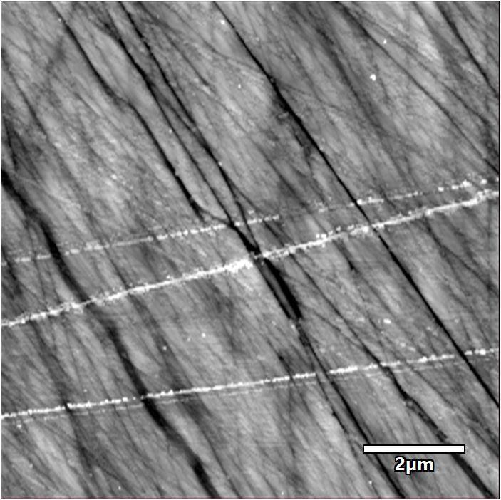
Figure 1. AFM image: unpolished substrate (Ra = 1.5 nm).
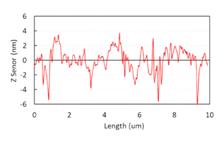
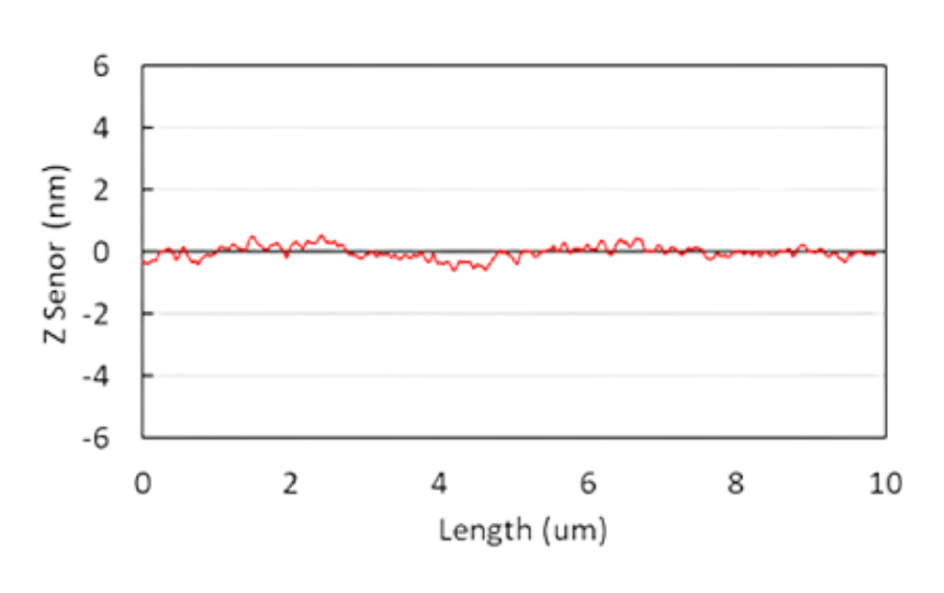
Figure 2. AFM image: after plasma polish (Ra = 0.70 nm).
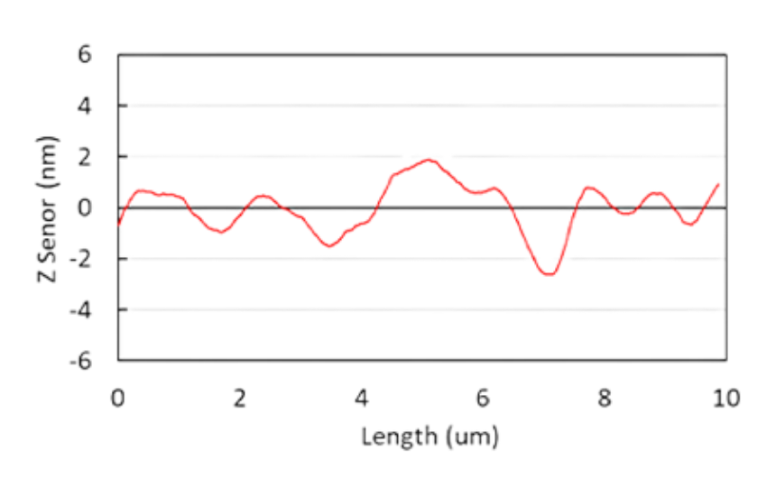
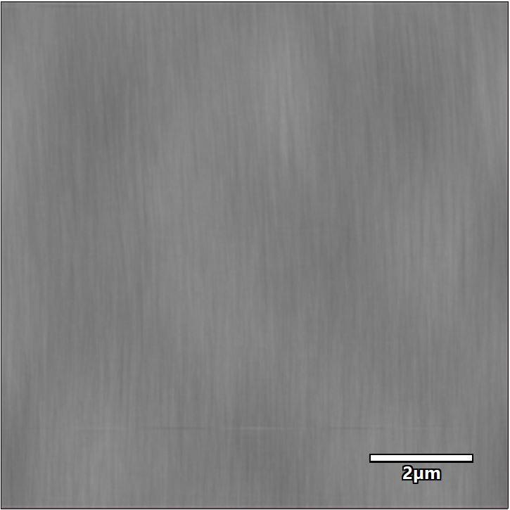
Figure 3. AFM image: SiC epi-layer on plasma polish wafer (Ra = 0.14 nm).
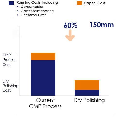
Using slurry components for the chemical mechanical processing can significantly increase the operational expenses. PPDE offers a very attractive lower opex and cleaner alternative to a costly and toxic chemicals intensive CMP process while approaching near zero wafer breakage levels
Oxford Instruments' plasma polish dry etch process enables thinner slicing industry roadmap to achieve increased wafers/boule further supporting the desired industry cost-down roadmap.
Clean water is recognised as becoming valuable and scarcer on a global scale, it is one of the key environmental issues of our lifetimes.
Plasma processing is standard within semiconductor HVM fabs with well established and controlled methods for handling of exhaust gases to strict environmental standards. The water used for plasma processing is the fab recirculation supply which is constantly recycled and re-used.
CMP requires large amounts of water to dilute and dispose of the slurry and toxic chemical effluent resulting from the process, a large cost and complexity when running large HVM cleanroom facilities.
150 mm SiC wafers are standard now and industry is moving to 200 mm in the near future. Our process is scalable, offering the same results to the SiC substrates independent of the size of the wafer. Moving to larger wafers sizes favours single wafer processing over batch processing. This allows industry standard methods of wafer handling, monitoring and control to be applied reducing touch-time, increasing yield and efficiency.
Wafer grinding and CMP require a series of steps utilising varying grit to improve the surface quality. This chemical mechanical process causes strain on the substrate increasing breakage and wafer loss. The particles leave scratches on the surface as it scrapes the SiC. Plasma polish dry etching is a contactless process using ionised gas to remove the silicon carbide selectively, providing high surface quality and minimise substrates damage.

Plasma polish dry etching replaces the CMP method in SiC process line.
*Orange processes show solutions covered by Oxford Instruments Plasma Technology.
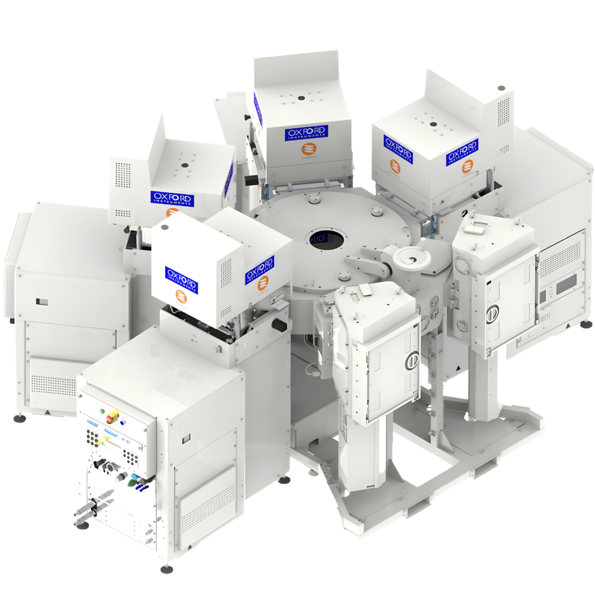
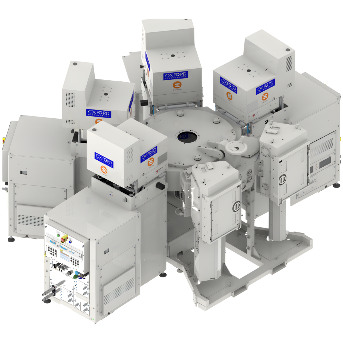
Platforms may be clustered to combine technologies and processes with either cassette or single wafer loading options. Hexagonal or square transfer chamber configurations are available.
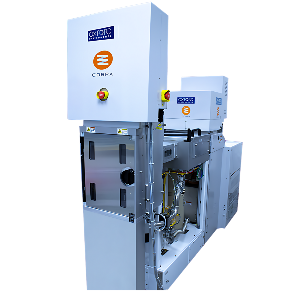
PlasmaPro 100 Cobra™ load-lock
Cobra twined-cassette cluster
Oxford Instruments is committed to providing a comprehensive, flexible and reliable global customer support. We offer excellent quality service throughout the life of your system.
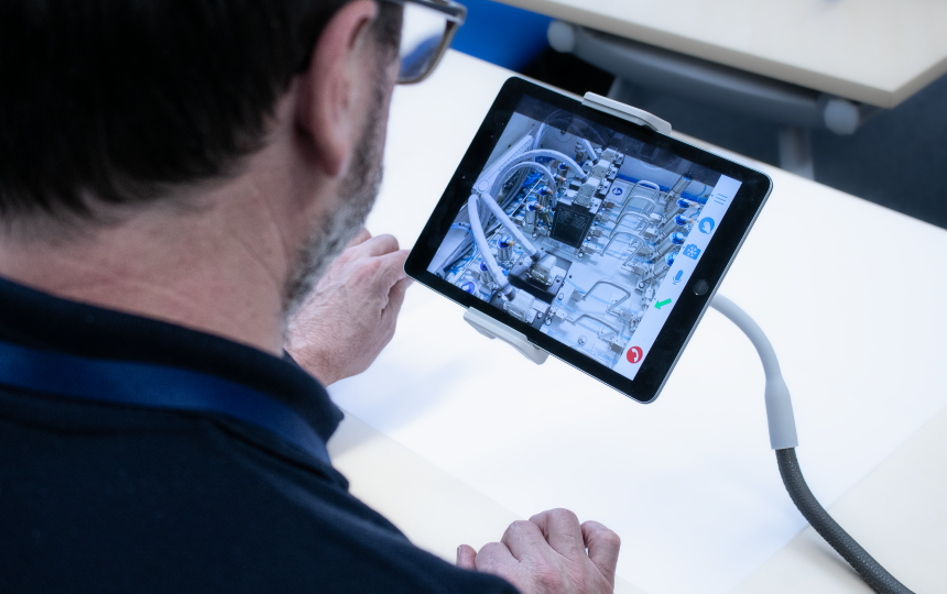
PTIQ is the latest intelligent software solution for PlasmaPro and Ionfab processing equipment.
At Oxford Instruments Plasma Technology, we offer a wide range of technical training courses designed to suit all skill levels and needs.

© Oxford Instruments 2026