 Part of the Oxford Instruments Group
Expand
Collapse
Part of the Oxford Instruments Group
Welcome to the second issue of Semi Interface magazine. We are once again joined by technology experts from around the globe, who in this issue share fascinating insights into the world of optoelectronics and datacoms.
Our authors dive into the current monumental changes that the datacom market is experiencing and discuss the tech advancements needed to keep up with exponentially increasing demand for data transceiving devices. Datacom, microLEDs, augmented reality, and more market and technology expertise is shared in this magazine, and you can get your FREE COPY below.
Download Magazine
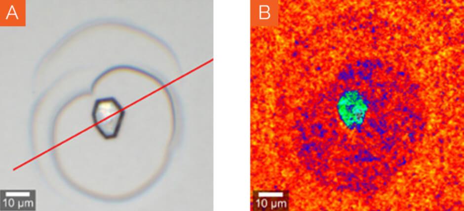
Damon Strom, Dr Judith Beer and Thomas Meyer from Oxford Instruments discuss the importance and value of Raman analysis when it comes to understanding compound semiconductor material properties. They share intriguing results from multiple investigations on various materials, and give insights through 2D and 3D visualisations.
As the world becomes more driven by datacentre requirements and AI applications, Dr‑Eng. S.K. Murad, Technology Consultant and Managing Director, looks to the future of InP wafers. He explores 6-inch InP scalable wafer fabrication, the challenges it generates, and the road ahead towards global adoption of 6-inch wafers and beyond.

“transitioning to 6‑inch InP wafers positions companies competitively within the semiconductor landscape.”
Robert Quinn is the Product Marketing and Business Development Expert at Quinns Media, He discusses how the immense growth in data traffic is bringing datacentres around the world to their functional limits, but how the implementation of cryogenic SOI CMOS transistors could help revolutionise the future of datacoms.

“A groundbreaking technology – cryogenic SOI CMOS transistors – may hold the key to revolutionising the future of data centres and quantum computing.”
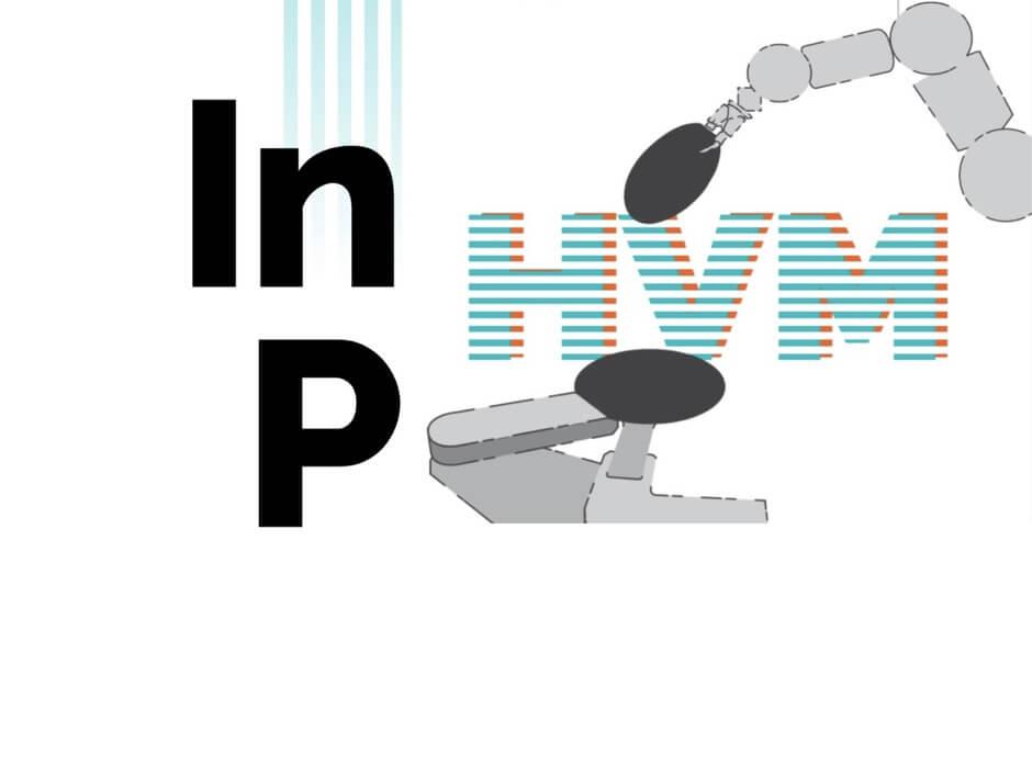
A collaboration between the application and marketing team at Oxford Instruments, Dr Ligang Deng, Dr Reasat Fahim and Dr Emma Coleman discuss the current datacom boom and its need for industrial automation. In order to keep up with the avalanche of technological advancements, including AI and autonomous driving, we must find ways to enhance both the quality and quantity of datacentre infrastructure - and InP has a big role to play.
Technology and Market Analyst, Dr Raphaël Mermet‑Lyaudoz from Display at Yole Group, shares with us his expert insights into the world of augmented reality (AR). More specifically, he speaks about vertical and slanted gratings for AR, and the application of AR headsets with microLEDs.

"The most recent microLED microdisplays can deliver millions of nits in very small packages."
Dr Ezgi Dogmus, is an Activity Manager Compound Semiconductors, at Yole Group rounds off the series with her expert analysis about the future of datacom, and what we should expect to see in the coming years. She speaks about how InP leadership over GaAs in the photonic compound semiconductor substrate market is influencing market trends today, and will continue to do so for some time, as we face this new era of the datacom boom.

"For InP, the AI boom is driving demand to transition from mainstream 3-inch substrates directly to 6-inch."
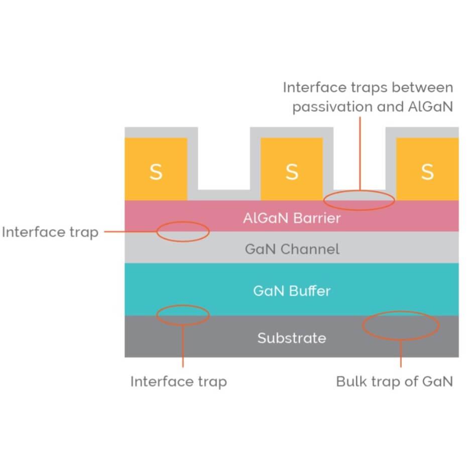
Dr Ehsan Azad, Senior RF & Microwave Engineer at CSA Catapult shares his specialist knowledge on GaN power amplifiers, the possible bridge between RF and photonics. With such versatility in its applications, Dr Azad discusses how high performing, lower consuming and reliable devices can be achieved with the help of GaN technology.
Welcome back to part two of this fascinating and enjoyable interview between Dr Aileen O'Mahony, Atomic Scale Processing Product Manager at Oxford Instruments, and Prof. Paul Hurley, Head of the Nanoelectronic Materials and Devices Group at Tyndall National Institute and the META Chair of Semiconductor Technologies in the School of Chemistry at University College Cork. In the last issue, they discussed the history of Si and the importance of all things interfaces. In this issue, they look at the present day and towards the future, discussing materials beyond Si and some of the work done by Prof. Hurley’s research group at Tyndall.

"This interfacial transition layer means that a clearly defined interface, where all dominant defects reside, is no longer valid."
Our Executive Director Klaas Wisniewski had the privilege to speak with Dr Chuck Mattera, former Chair and CEO at Coherent Corp. Chuck was very generous with his time and shared his thoughts, looking back on his esteemed career, managing for high performance in business, and where the datacom market will progress in the future.

Dr Chuck Mattera
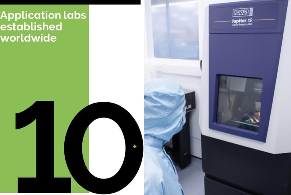
Dr Christian Lang, Managing Director of the Materials Analysis Business at Oxford Instruments, kindly sat down with us to share his expert knowledge about advanced metrology methods, and how it is a vital component of next-generation semiconductor manufacturing. From electron backscatter diffraction to atomic force microscopy to Raman spectroscopy, Dr Lang speaks of the importance of material analysis and how Oxford Instruments provides customers with a wide range of standout metrology products.
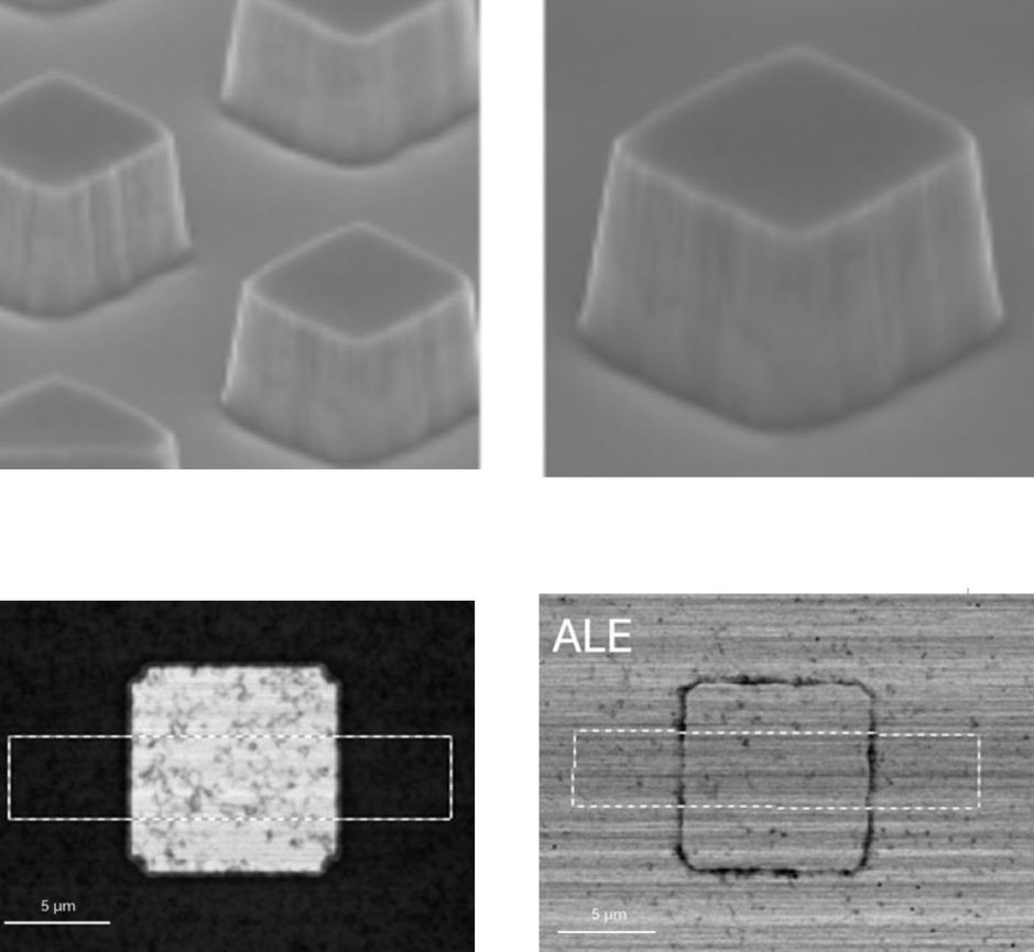
Dr Andrew Newton, New Product Solutions Manager for Oxford Instruments Plasma Technology, explores the possibilities that atomic layer etching (ALE) can bring to the world of tech, with a focus on microLEDs. Sidewall smoothness is imperative when it comes to high performance devices, and isotropic ALE has been achieving attractive results that may hold the key to success.
In our final article, we dip our toes into the topic of our next Semi Interface issue - Quantum Technology. Dr Wladick Hartmann, Co-Managing Director and CTO at Pixel Photonics, discusses the revolutionary superconducting nanowire single‑photon detectors (SNSPDs) and how their exceptional performance characteristics can be utilised in photonic integrated circuits (PICs). He speaks about some the incredible work that Pixel Photonics is working on, and their commitment to help building the future of quantum, and beyond.

"At Pixel Photonics, we specialise in developing waveguide-integrated SNSPDs, devices that have set a new benchmark for single‑photon detection."

© Oxford Instruments 2026

