 Part of the Oxford Instruments Group
Expand
Collapse
Atomic Layer Etching (or ALE) is an advanced etch technique that allows for excellent depth control on shallow features. As device feature size reduces further and further ALE is required to achieve the accuracy required for peak performance.
High fidelity pattern transfer (etching) is essential for the fabrication of today’s advanced microelectronic devices. As features shrink to sub-10nm levels, and novel devices make use of ultra-thin 2D materials, there is an increasing need for atomic-scale fidelity.
This has led to a growing interest in a technique known as Atomic Layer Etching (ALE), which overcomes the limitations of conventional (continuous) etching at the atomic scale. Plasma-based atomic layer etching is a cyclical etching process of gas dosing and ion bombardment that removes material layer by layer and has the potential to remove single atomic layers with very low damage.
Achieves etching of layers with high depth accuracy
Advanced technology for high control of etch depth
Low damage to underlying substrates
Can be used in combination with standard ICP
Atomic Layer Etching typically involves a cycle of 4 steps that is repeated as many times as necessary to achieve the required etch depth. This example shows ALE of AlGaN etching with Cl2/Ar.
Step 1) Dosing of the substrate with an etching gas, which adsorbs on and reacts with the etch material. The etch gas is often plasma dissociated to enhance the rate of adsorption. With the correct choice of dosing gas and parameters, this can be self-limiting, if the chemical dose stops after adsorbing one monolayer.
Step 2) Purging of all residual dose gas.
Step 3) Bombardment of the surface with low energy inert ions which removes the reacted surface layer. This can be self-limiting if the energy of the ions is sufficient to remove the chemically modified layer, but insufficient to (sputter) etch the underlying bulk material.
Step 4) Etching products are purged from the chamber.

Read our article in Compound Semiconductor
Atomic layer etching promises to improve the quality of GaN-based HEMTs and eradicate the damage associated with high etching rates.
Written by Dr Mike Cooke and Dr Andy Goodyear for Compound Semiconductor magazine.

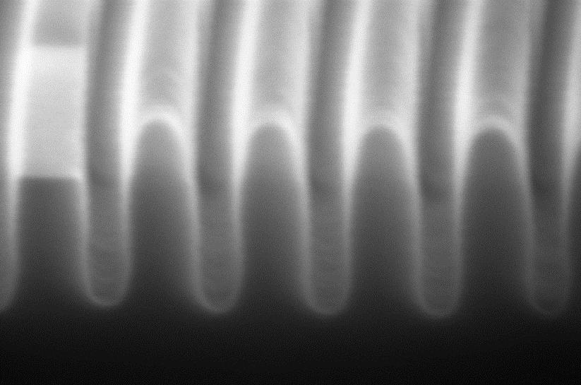
25nm wide Si trenches etched to 110nm depth by ALE, HSQ mask still in place.

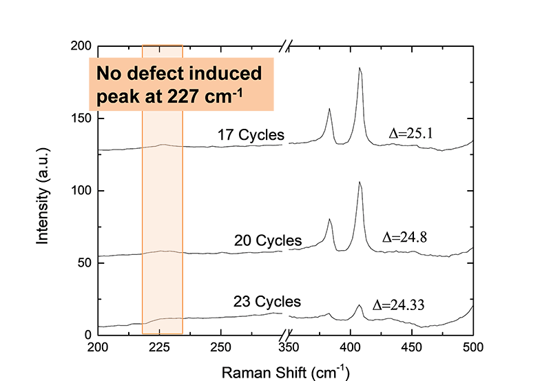
ALE of MoS2 shows no Raman defect peak after etching, highlighting the low damage etching capabilities of ALE.

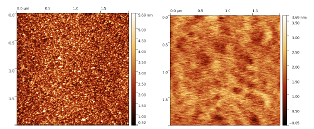
AlGaN surface roughness after 200 ALE cycles, left = before etching (Ra = 600pm), right = after etching (Ra = 300pm). The surface has been smoothed by ALE.
ALE is suitable for a wide range of materials, including Si, a-Si, MoS2, SiO2, GaN, AlGaN, III-V’s, Si3N4, graphene, HfO2, ZrO2, Al2O3, metals etc.
Material Etched |
Dose Gas |
Etch Gas |
MoS<sub>2 |
Cl<sub>2 |
Ar |
Si or a-Si |
Cl<sub>2 |
Ar |
SiO<sub>2 |
CHF<sub>3</sub> or C<sub>4</sub>F<sub>8 |
Ar or O<sub>2 |
AlGaN or GaN |
Cl<sub>2</sub>, BCl<sub>3 |
Ar |
AlGaN or GaN |
N<sub>2</sub>O |
BCl<sub>3 |
GaAs or AlGaAs |
Cl<sub>2</sub>, BCl<sub>3 |
Ar |
InP or InGaAsP etc. |
CH<sub>4</sub>, Cl<sub>2 |
Ar |
SiN |
H<sub>2 |
Ar |
Al<sub>2</sub>O<sub>3 |
BCl<sub>3 |
Ar |
Graphene |
O<sub>2 |
Ar |
HfO<sub>2</sub>, ZrO<sub>2 |
Cl<sub>2</sub>, BCl<sub>3 |
Ar |

AlGaN ALE Process Cycle

AlGaN Etch per Cycle with and without Chlorine dose
Our Atomic Layer Etching equipment is built on 13+ years of experience. Key features include: