

Oxford Instruments enables ROHM’s in-house GaN manufacturing with…
Oxford Instruments, a leading provider of advanced plasma processing solutions…
 Part of the Oxford Instruments Group
PECVD is a well established technique for deposition of a wide variety of films. Many types of devices require PECVD to create high quality passivation or high density masks.
Our PECVD systems are specifically designed to produce excellent uniformity and high rate films, with control of film properties such as refractive index, stress, electrical characteristics and wet chemical etch rate. Our plasma cleaning process with end-point control removes or reduces the need for physical/chemical chamber cleaning.
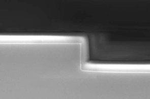
PECVD of TEOS SiO2
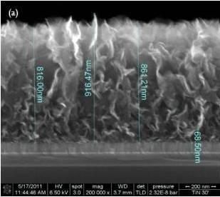
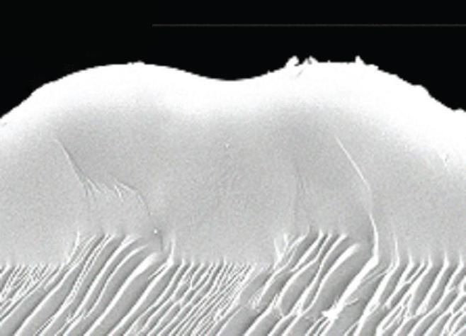
PECVD of vertically aligned graphene (Courtesy of IMEC, Belgium)
The PlasmaPro 100 PECVD system is specifically designed to produce high quality films with excellent uniformity and control of film properties such as refractive index, stress, electrical characteristics and wet chemical etch rate. Our cutting-edge PECVD system is suitable for dielectric films passivation (e.g. SiO2, SiOxNy), silicon carbide, amorphous silicon, hard mask deposition and anti-reflective coatings.
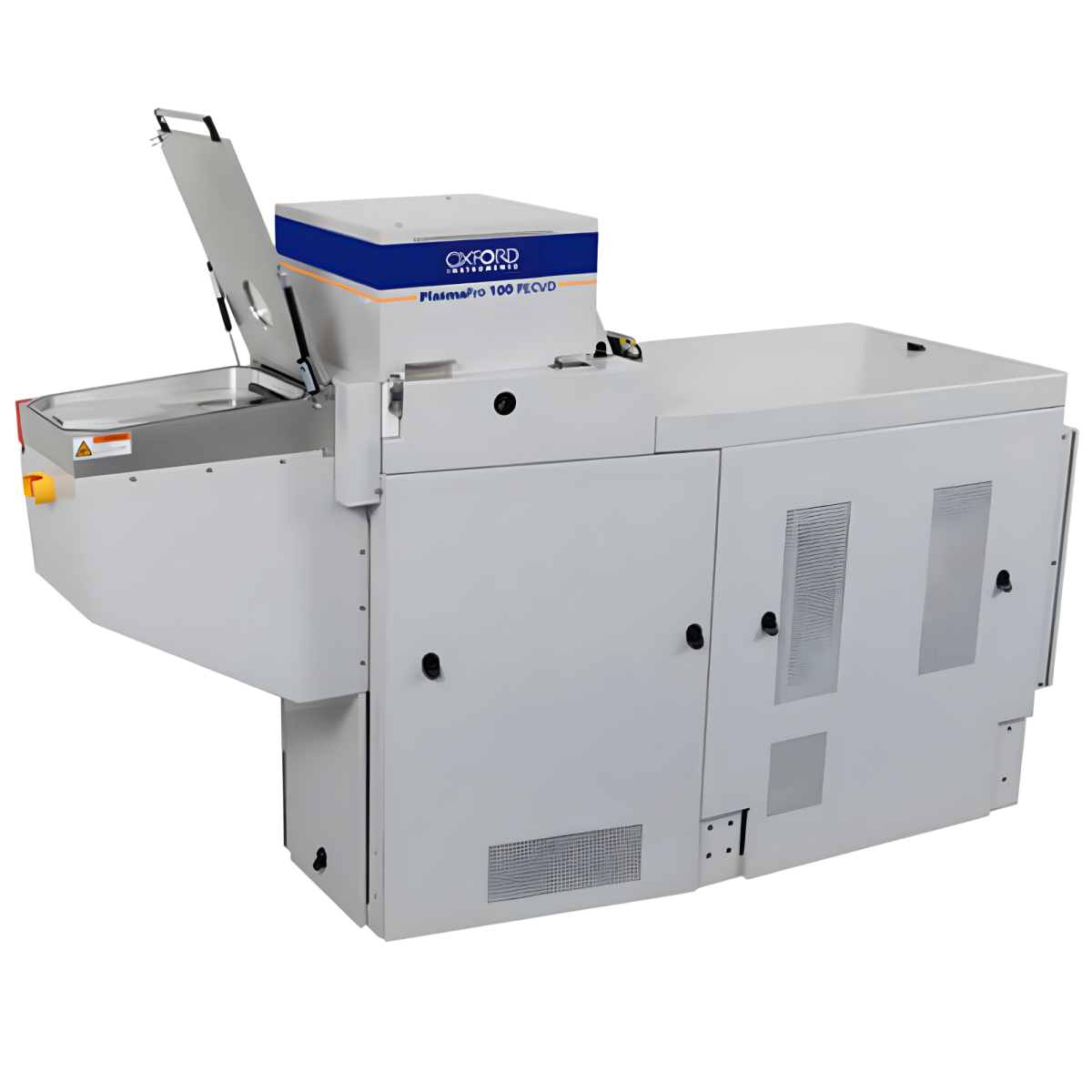
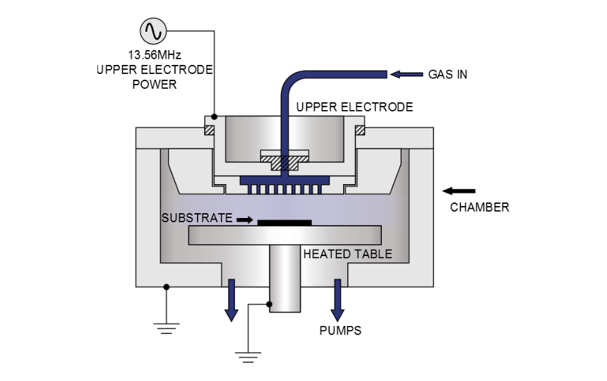
PlasmaPro 100 PECVD delivers excellent conformal deposition and low particle generation due to electrode temperature uniformity and shower head design in the electrode, allowing RF energy to produce the plasma.
The high energy reactive species of plasma offers high deposition rates to achieve the desired thickness of the substrate while maintaining low pressure. Its dual frequency 13.56 MHz and 100 KHz power applied to upper electrode enables stress control and film densification.
High rate SiO2 PECVD
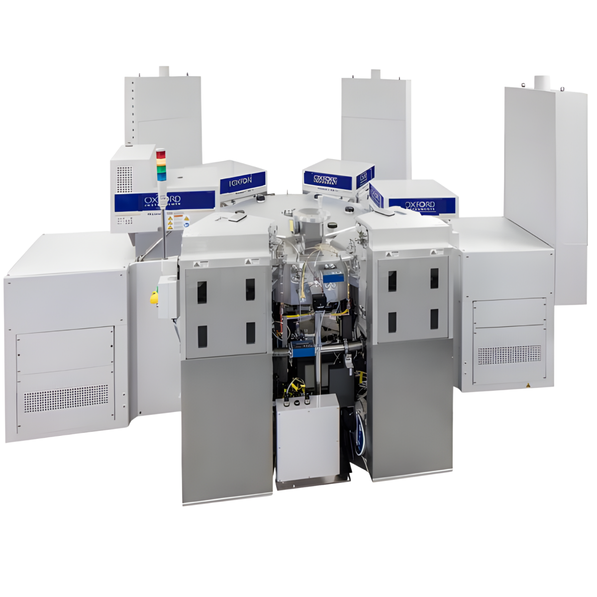
Clustering of up to 4 process modules
Resistive heated electrodes: up to 400 °C or 1200 °C
Precursor delivery option:
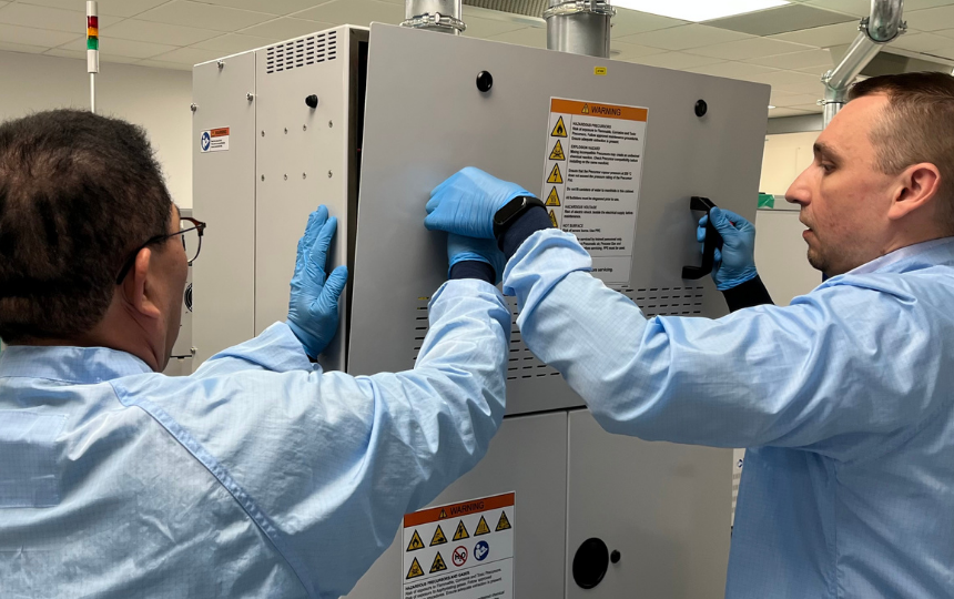
Oxford Instruments is committed to providing a comprehensive, flexible and reliable global customer support. We offer excellent quality service throughout the life of your system.
PTIQ is the latest intelligent software solution for PlasmaPro and Ionfab processing equipment.
At Oxford Instruments Plasma Technology, we offer a wide range of technical training courses designed to suit all skill levels and needs.

© Oxford Instruments 2026