 Part of the Oxford Instruments Group
Expand
Collapse
Part of the Oxford Instruments Group
MicroLEDs are an emerging display technology with strong technical differentiation. MicroLED displays can achieve high brightness, contrast and dynamic range with low power consumption. These benefits make the technology ideally suited for applications such as Augmented Reality and smartwatch displays. In order to meet the high-volumes demanded by the consumer market, the manufacturing process of microLED has to be optimized for yield and throughput.
With many years experience in plasma processing, Oxford Instruments provides innovative solutions for red, blue and green LEDs. The solution portfolio includes processing of III V material such as GaN or InGaAlP, as well as deposition processes such as ALD of Al2O3. We enable the world’s leading semiconductor companies and scientific research communities to manufacture high efficiency, low cost mini and microLEDs.
DOWNLOAD BROCHURE


Simplified process flow. Orange processes show solutions covered by Oxford Instruments' technology.
We provide proven, innovative solutions including plasma etching and deposition for small die size and narrow pitch microLEDs. Our solutions include processes such as die singulation and ALD of dielectrics for electrical passivation. Our dielectric passivation is ideally suited for fine pitch designs and delivers reliable device operation with minimal crosstalk between pixels whilst maximising external quantum efficiency.

Dr Fang, Deputy Division Director, Electronics and Optoelectronics System Research Laboratories
“Their solutions, unrivalled local process support and their capability to nurture laboratory developments into production standards with our industrial partners were key influences in our purchase decision”.
For optimum brightness and efficiency of microLEDs, Oxford Instruments have demonstrated high-quality gallium nitride (GaN) etching solutions for green and blue microLEDs with excellent process repeatability.
High quality GaN etching supports microLED manufacturers in delivering high device efficiency. Our plasma etching process delivers excellent surface quality on GaN devices with clean, smooth sidewalls and feature base surfaces.
ICP etched mesas achieve the ultimate surface quality required for high performance AlGaInP devices (Red microLED). Collaborating with key microLED players worldwide, we have proven expertise to deliver process results for backside via, sloped features and vertical mesa/isolation for microLED applications.
Atomic layer etching (ALE) is an advanced technology capable of etching layers with high depth accuracy and low damage. It is applicable in combination with conventional ICP etch processing to high performance GaN mesa etch and low damage contact pad opening.
CAIBE (Chemically Assisted Ion Beam Etching) can also be used for mesa etching. CAIBE provides excellent control of sidewall angle and high selectivity (albeit at a lower etch rate when compared with ICP etch). IBE technology has also been demonstrated to be ideal for metal contact etch with minimal or no damage to the microLED structures.
Sidewall passivation has been identified as a critical step in the fabrication of microLEDs. High quality deposition is required to demonstrate optimal sidewall quality and maximise the device efficiency. Atomic Layer Deposition has been proven as a solution to help minimise non-radiative recombination which is present as a result of etch damage.
Our high-quality passivation utilizes surface pre-treatment for superior interface control, improving devices’ optical performance, as well as a low ion energy plasma source for low damage deposition. Our solution portfolio includes advanced processing for a range of material including SiN, SiO2, AlN, HfO2 or Al2O3. The Atomfab is specifically manufactured to deliver high quality PE-ALD films at market leading throughput, yield and cost of ownership.
High-quality materials are also required for dielectric encapsulation and electrical contact deposition. Our Ion Beam Deposition technology delivers materials with high purity, high density and low surface roughness, ideal for microLEDs.
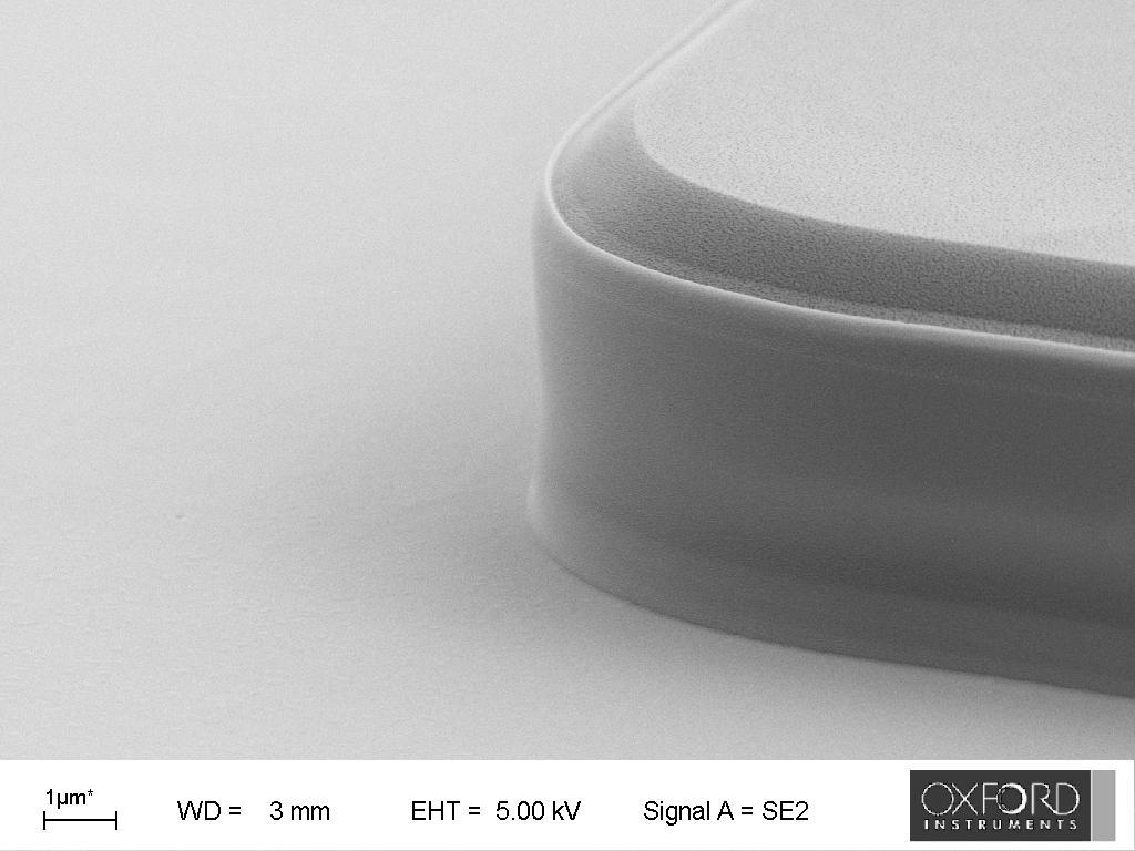
GaN Etch with smooth surface
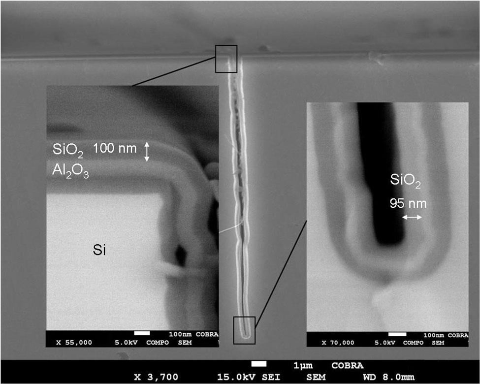
ALD in SiO2 - Courtesy by Eindhoven University of Technology
Cobra's uniform plasma source delivers excellent control for III V material processing including GaN and AlGaInP layers used in microLED. Our ICP etching system provides proven reliability with high throughput for maximum yield and low CoO.
DOWNLOAD BROCHURE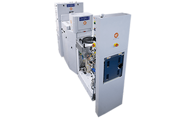
Atomfab enables microLED companies to adopt advanced material technology for high volume production. Its proprietary new plasma source delivers significant CoO reduction, increased yield and excellent film quality & device performance.
DOWNLOAD BROCHURE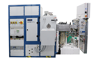
Ionfab delivers excellent uniformity and repeatability. Ion energy and angle of incidence control combined with precision SIMS end point enable the etching of vertical walls with accurately controlled depth and low wall damage. Ionfab offers deposition of high quality, dense and smooth surface films with ultra-low contamination.
DOWNLOAD BROCHURE
© Oxford Instruments 2026

