Part of the Oxford Instruments Group
Expand
Collapse
Part of the Oxford Instruments Group
Quantum Technology refers to the next generation of computing, communication, simulation and sensing technology that relies on two key features of individual atoms, electrons or light particles (photons): superposition and entanglement.
Superposition allows these quantum systems to live in multiple states at once, while entanglement allows them to be co-dependent, enabling the possibility of connecting them in a network while still acting as one system.
Understanding the mechanics of the Quantum world at the turn of the century enabled some of the most widely used technologies today such as the flash memory, superconductors, lasers and LEDs. Today, we are seeing the evolution of a new generation of quantum devices that goes beyond the exploitation of quantum effects and relies on the manipulation of quantum states.
Quantum technology is now enabling a new generation of photonics and electronics applications from quantum computing to solve seemingly intractable problems, sensors for navigation, atomic clocks and secure data communications.
This fast-evolving field of technology demands a wide range of quantum materials processes for high precision device fabrication.
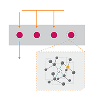
Oxford Instruments Plasma Technology provides state of the art materials deposition and etching processes for quantum technology R&D and device development. Using our strong expertise in plasma etching and deposition of materials, we enable researchers and engineers to work with a wide range of materials and build critical quantum device components such as single-photon detectors, quantum interconnects, tunnel junctions, integrated quantum optics/photonics, Nitrogen vacancy centres, and more.
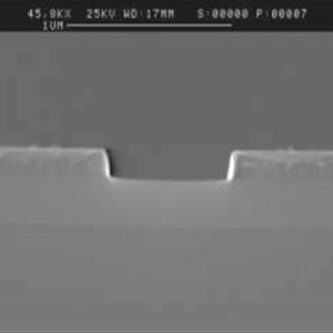
20nm Nb etched down to SiO2 using RIE
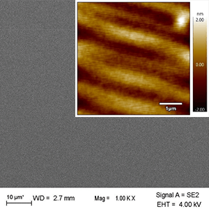
Defect-free clean & smooth diamond surface post 16µm etch
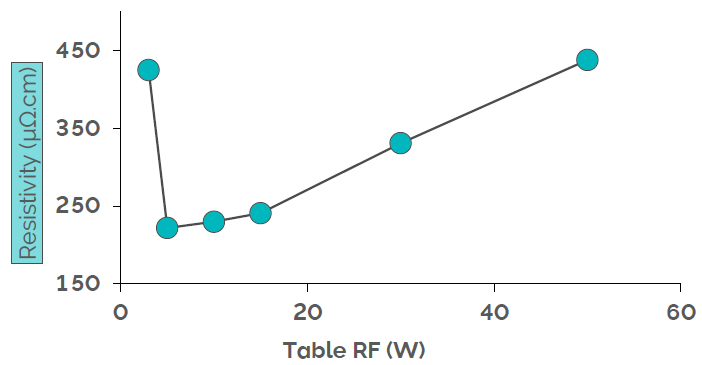
Adding a small amount of bias improves the resistivity of the NbN film.
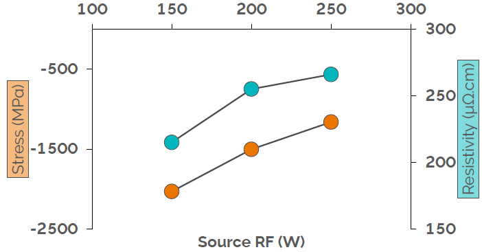
Varying the plasma power is another way to adjust the stress of the deposited NbN.
Need more information?
CONTACT US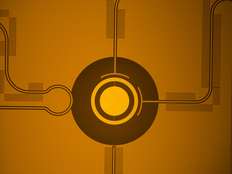
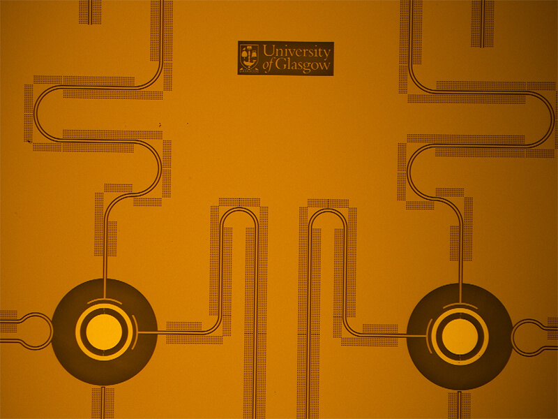
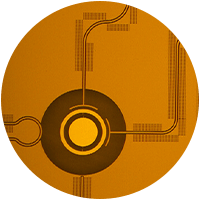
Superconducting qubits and resonators fabricated using PlasmaPro 100 RIE.
(Courtesy of University Glasgow)
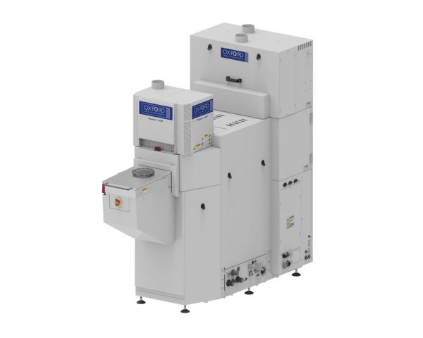
Our PlasmaPro 100 platform enables high precision deposition and etching of a wide range of materials for quantum devices. We offer key processing solutions for various device fabrication challenges for the various approaches in today’s quantum technology R&D and device development.
Oxford Instruments have a strong history in providing state of the art solutions in this rapidly developing applications are a key enabler of quantum technologies beyond device fabrication solutions.
Find out more about all of our Quantum solutions.
OUR SYSTEMS
© Oxford Instruments 2026