Part of the Oxford Instruments Group
Expand
Collapse
Part of the Oxford Instruments Group
We offer three key applications for photonic integrated circuits for quantum:
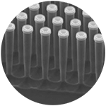
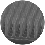
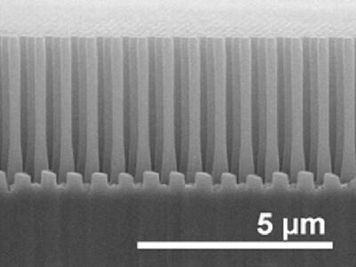
We propose a range of cryogenic etch processes to fabricate optical components such as gratings, ring resonators, optical filters, delay lines and waveguides, made from Si/Si3N4. These are key building blocks of a Quantum Computer, enabling light coupling into the chip, photon manipulation and transport down to single photon detectors.
Our cryogenic etch processes are characterized by:
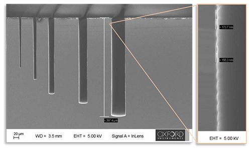
Bosh etched structures
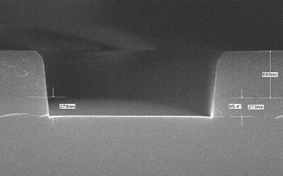
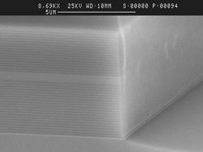
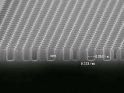
SiNx cryo etch
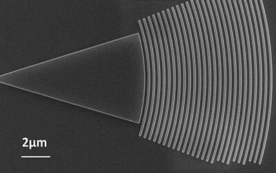
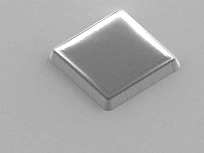
Grating coupler on SOI
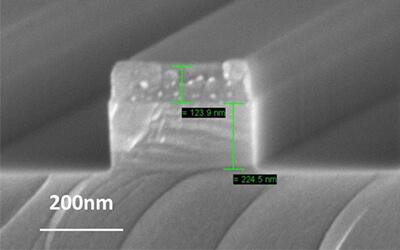
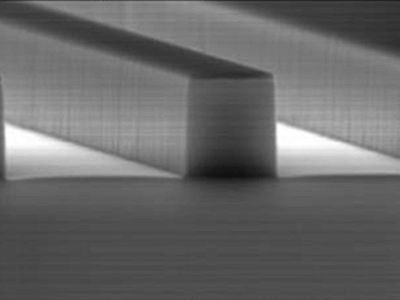
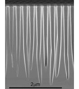
Cryo etched SOI waveguide
Minimal scallop size | |||||||||
Etch rate |
> 3 μm/min | ||||||||
Profile |
90 ±0.5° | ||||||||
Selectivity |
> 45:1 | ||||||||
Scallops |
< 35 nm | ||||||||
Depth |
22 μm | ||||||||
AR |
≈ 11 | ||||||||
Smooth sidewalls | |||||||||
Etch rate |
> 2 μm/min | ||||||||
Profile |
91° | ||||||||
Selectivity |
> 65:1 Si:SiO<sub>2</sub> | ||||||||
Sidewall roughness |
< 5 nm | ||||||||
Depth |
22 μm | ||||||||
AR |
≈ 6 | ||||||||
Curved profile | |||||||||
Etch rate |
> 190 nm/min | ||||||||
Profile |
Shaped | ||||||||
Selectivity |
> 12:1 | ||||||||
Sidewall roughness |
< 5 nm | ||||||||
Depth |
485 nmm | ||||||||
Pillar width |
≈ 105 nm | ||||||||
GaAs / AlGaAs Heterostructures
InP Ridge Waveguide
GaN Photonics Crystal
GaAs / AlGaAs Photonic Crystal
InP Photonic Crystal
InSb / InSbAs
One of the greatest challenges with Si3N4 deposition for applications in waveguides is the in-film hydrogen content, typically coming from the precursors and leading to optical losses.
Therefore, we've developed a high-temperature PECVD process which shows a low concentration of hydrogen and enables enhanced stress control as well as a higher deposition rate, These make high-temperature PECVD of Si3N4 particularly suited for the fabrication of low-loss optical components.
Other approaches include ICP CVD using SiCl4 or low-temperature ICP CVD followed by in-situ anneal at temperatures above 1000°C in our PlasmaPro 100 Nano system (maximum temperature: 1200°C).
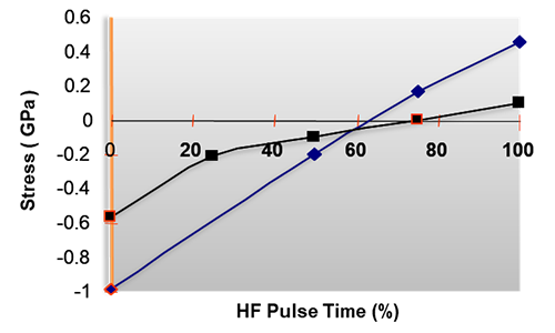
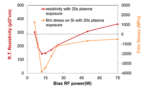
PECVD film stress control
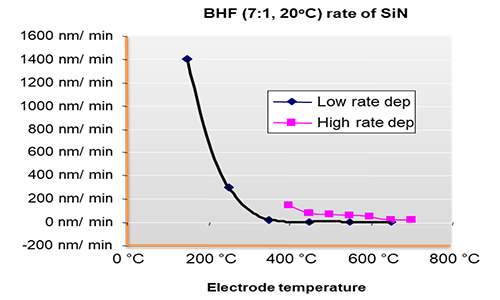
High temp PECVD with low BHF etch rate
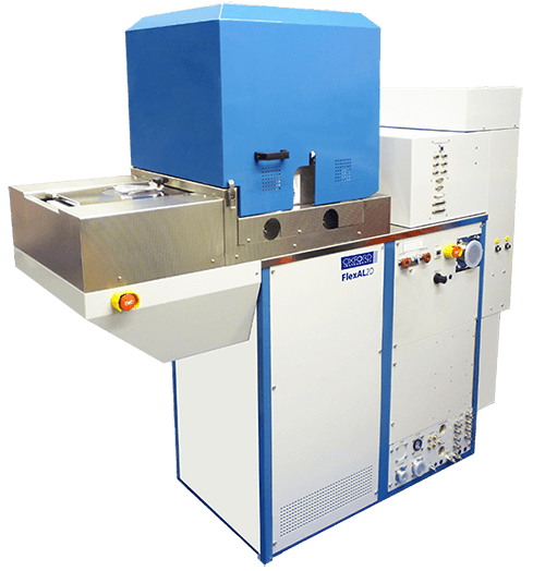
Enabling these solutions are the FlexAL and PlasmaPro 100 deposition and etch systems, capable of producing small coupons through to 200 mm wafers, clusterable to increase throughput and avoid vacuum breaks. Our PlasmaPro 100 platform enables high precision deposition and etching of a wide range of materials for quantum devices.
We offer key processing solutions for various device fabrication challenges for the various approaches in today’s quantum technology R&D and device development.
Oxford Instruments have a strong history in providing state of the art solutions in this rapidly developing applications are a key enabler of quantum technologies beyond device fabrication solutions.

© Oxford Instruments 2026