Part of the Oxford Instruments Group
Expand
Collapse
Part of the Oxford Instruments Group
We offer a range of etch (ICP etch; RIE) and deposition (ALD; PECVD) solutions for diamond quantum applications. This includes thinning down diamond to improve the manipulation of NV centers, and structuring diamond to enable new applications in quantum information and sensing.
We offer three quantum diamond fabrication solutions:
A 3-step RIE process to bring the NV centers closer to the surface while providing additional protection via O-termination, thereby enabling improved manipulation or storing of quantum information.
1) Isotropic particle removal
2) Diamond bulk etch with precise stop within a few um from the NV centres
3) Oxygen termination of the surface to improve stability of NV centers
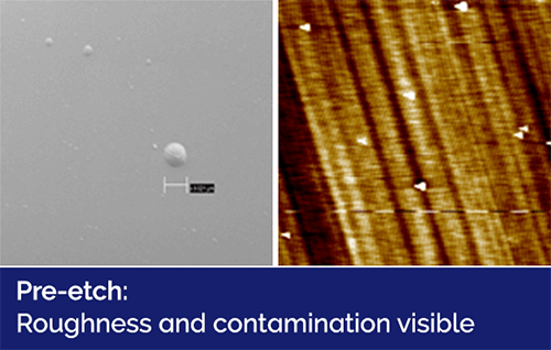
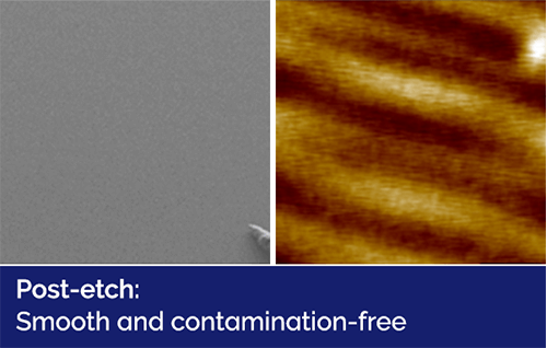
3-step RIE process to create a defect-free, smooth, O-terminated diamond surface.
Photonic crystals, nanocavities and waveguides coupled to quantum emitters, to improve photon generation, increase light extraction and allow for long-distance transport of quantum information.
Optomechanical microdisk resonators to enhance spin-photon coupling, enable greater manipulation of quantum information and offer an interface to various quantum platforms.
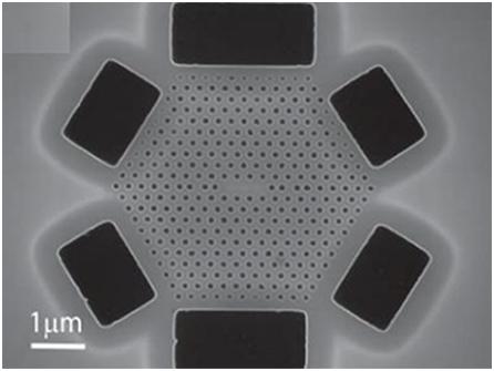
Photonic crystals in Diamond
(Credit: S. Bogdanovic, TU Delft)
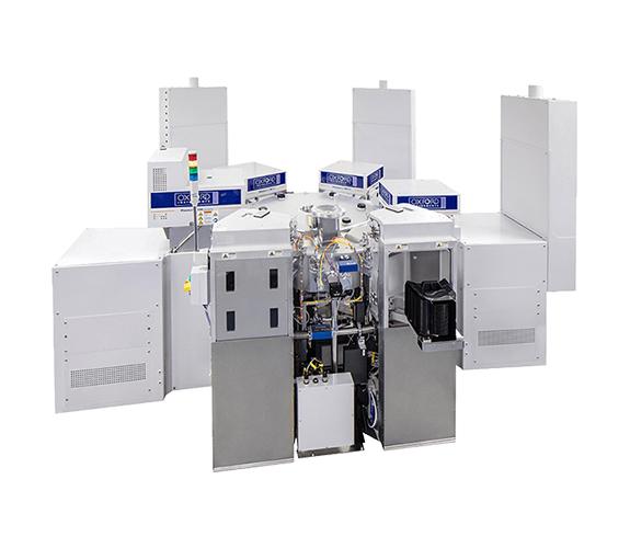
Our PlasmaPro 100 platform enables high precision deposition and etching of a wide range of materials for quantum devices. The FlexAL atomic layer deposition (ALD) system offers a broad range of optimised high-quality ALD processes.
Our PlasmaPro 100 RIE can rapidly etch through the bulk material while ensuring a controlled and residue/contamination free surface, with very low roughness (typically below 3A) to limit noise and optical losses, and oxygen terminated to provide additional protection to the shallow qubits.
We offer key processing solutions for various device fabrication challenges for the various approaches in today’s quantum technology R&D and device development.


© Oxford Instruments 2026