Part of the Oxford Instruments Group
Expand
Collapse
Part of the Oxford Instruments Group
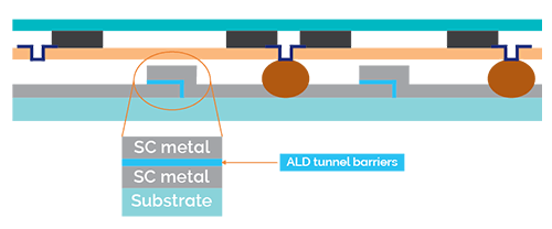
We offer several solutions for superconducting qubits & quantum circuits:
We've successfully deposited superconducting TiN by plasma ALD using bias to finely tune the film properties such as room temperature resistivity. Consequently, this has achieved a critical temperature of 3 K for a 90 nm film deposited at 250°C
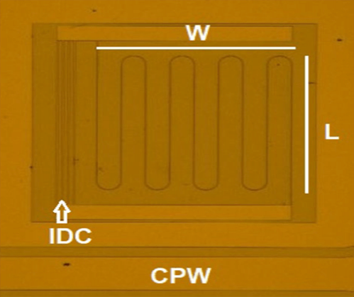
(Credit: University of Glasgow)
We've developed a plasma ALD process of NbN for higher temperature operation of superconducting interconnects
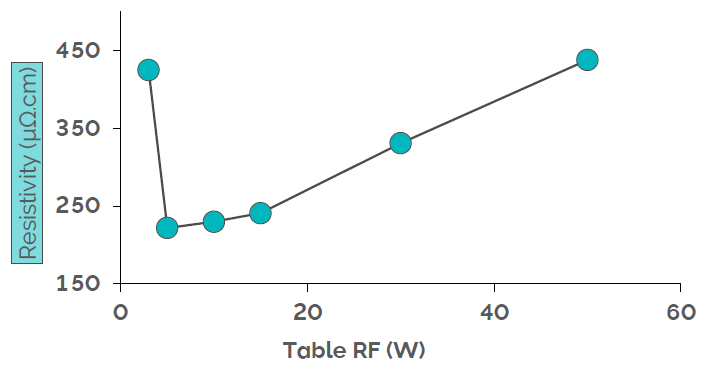
Adding a small amount of bias improves the resistivity of the NbN film.
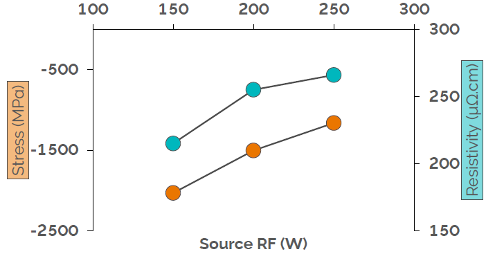
Varying the plasma power is another way to adjust the stress of the deposited NbN.
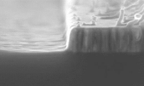
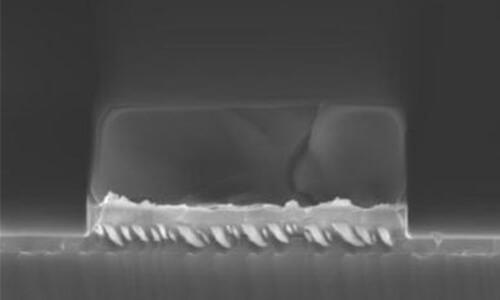
Single-layer or stack etch resulting in:
200 nm Nb etch
Resist mask fully stripped
200 nm Mo etch
Resist mask partly stripped
Vertical Al/Al2O3/Al tunnel junction stack etch
Combine the benefits of plasma ALD (PE-ALD) with the capability of clustering systems to other technologies and unlock unique capabilities.
Remove amorphous native oxide prior to growing high-quality PE-ALD of Al2O3 by either:
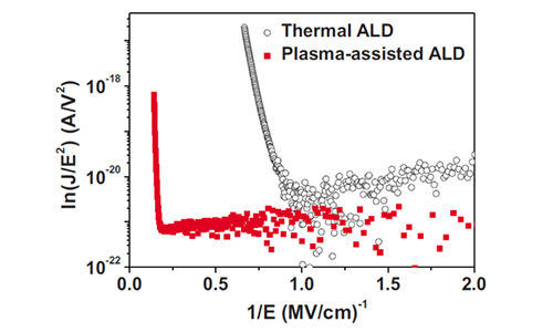
(Credit: Jinesh et al., 2011)
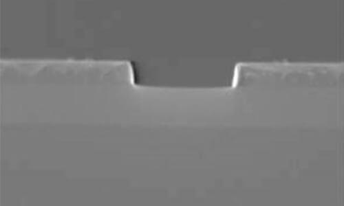
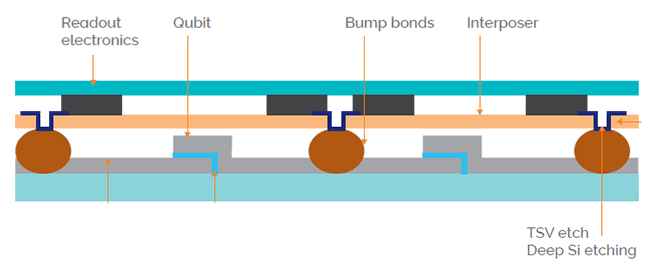
We offer two etch processes to fabricate vertical TSVs, thereby enabling scaling of superconducting quantum circuits based on a 3D architecture
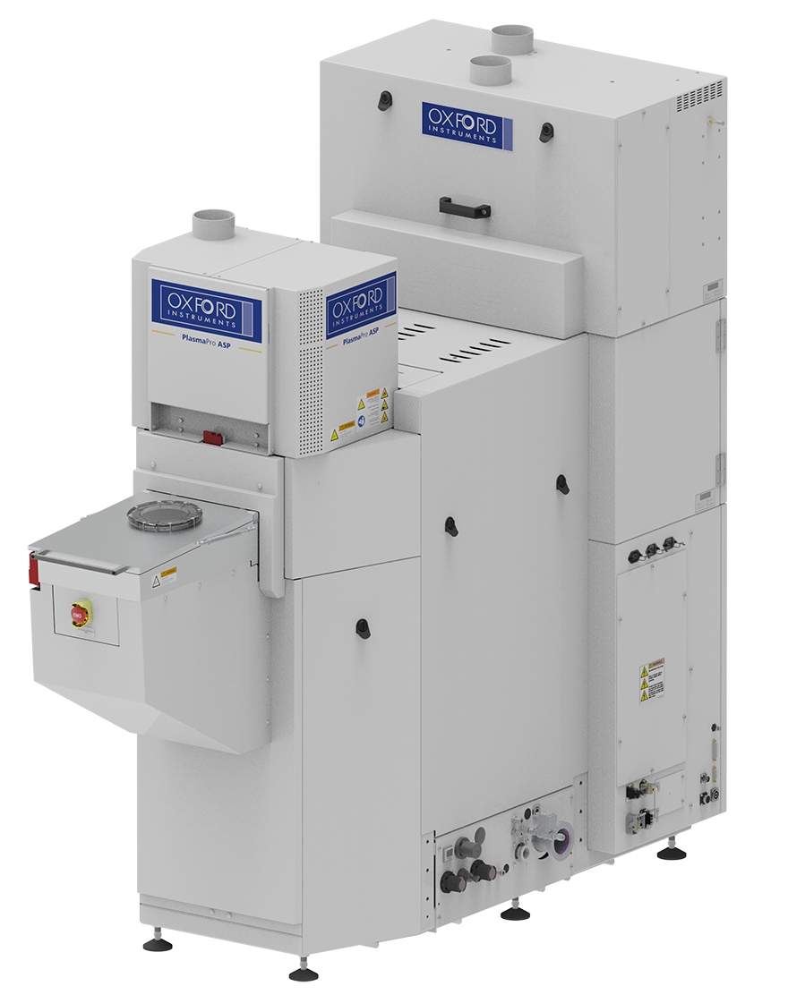
The PlasmaPro ASP Atomic Layer Deposition system enables deposition of conformal superconducting nitrides into TSVs at rates exceeding 25 nm/hour.
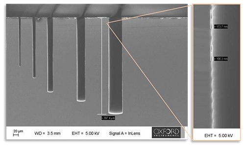
Bosch etch for TSV
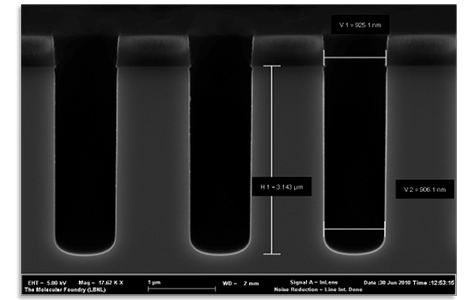
Cryo etch for ultra smooth sidewall features
Enabling these solutions are the PlasmaPro ASP and PlasmaPro 100 deposition and etch systems, capable of producing small coupons through to 200 mm wafers, clusterable to increase throughput and avoid vacuum breaks.
Our PlasmaPro 100 platform enables high precision deposition and etching of a wide range of materials for quantum devices.
The PlasmaPro ASP atomic layer deposition (ALD) system has been designed to ensure high quality materials that can be deposited at speed with flexibility to run multiple chemistries to give excellent layers for incorporation into devices. The PlasmaPro ASP has been added in the Atomfab® product range platform to deliver fast and low damage remote plasma enhanced ALD
Oxford Instruments have a strong history in providing state of the art solutions in this rapidly developing applications are a key enabler of quantum technologies beyond device fabrication solutions.

© Oxford Instruments 2026