

Oxford Instruments enables ROHM’s in-house GaN manufacturing with…
Oxford Instruments, a leading provider of advanced plasma processing solutions…
 Part of the Oxford Instruments Group
Designed to enable the fabrication of all Si etch devices, deep silicon etching delivers:
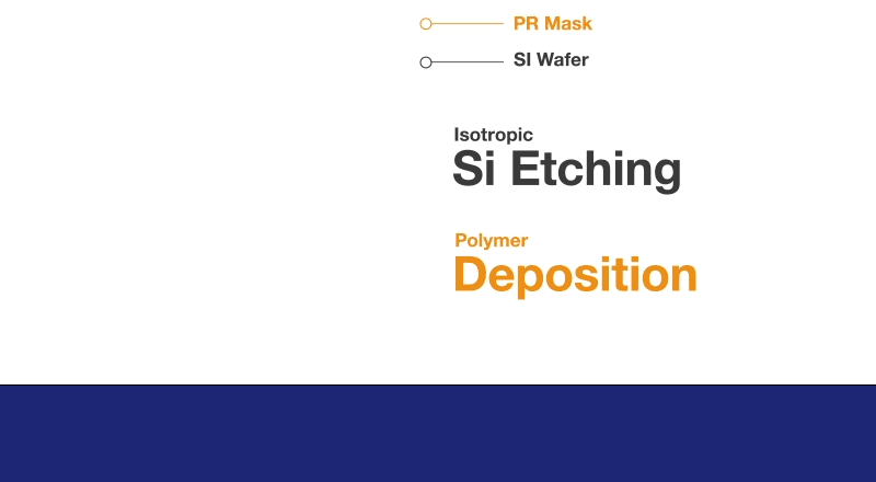
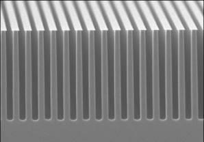
DRIE or Deep Silicon Etching (DSiE), is a highly anisotropic etch process used to create deep, steep-sided holes and trenches in wafers/substrates, typically with high aspect ratios.
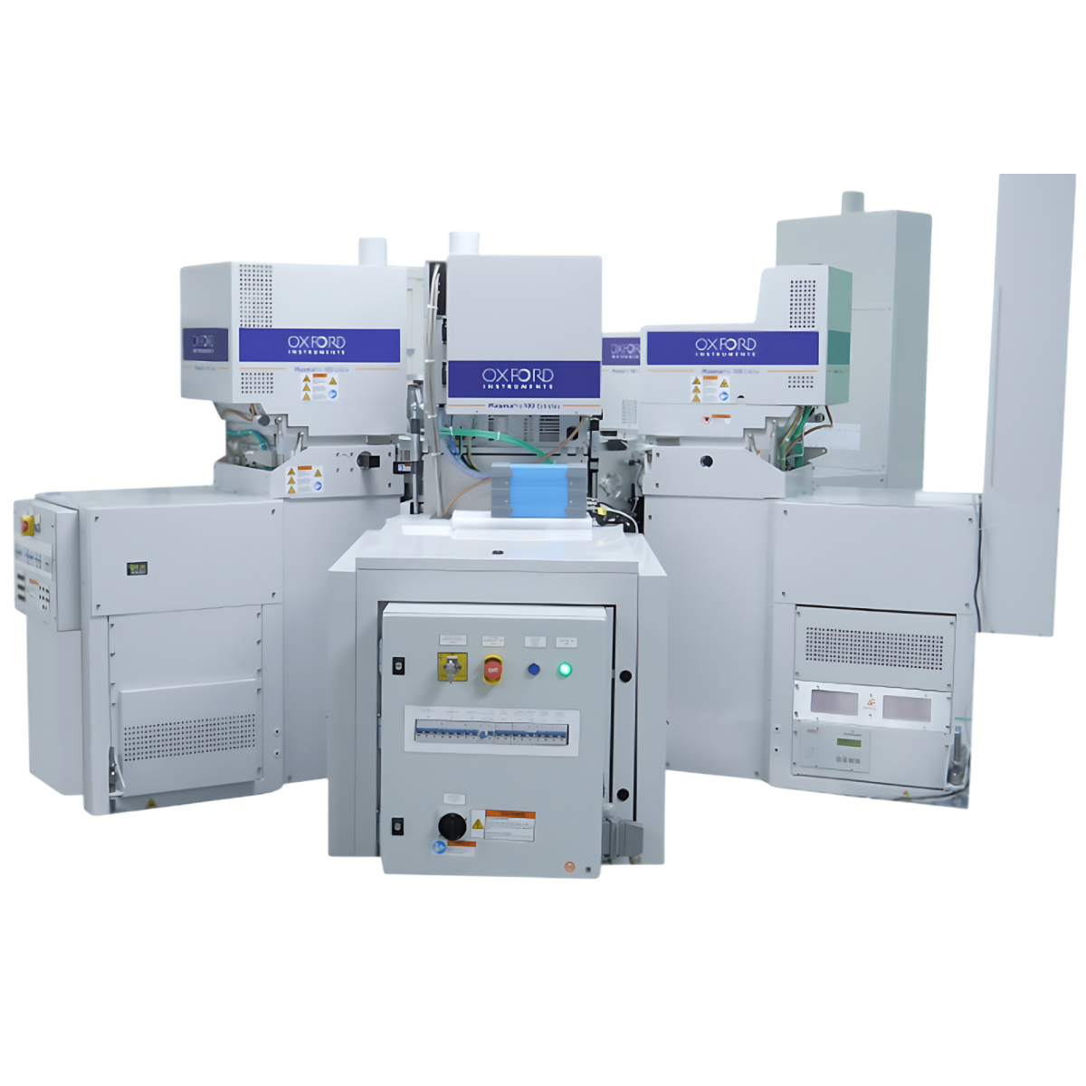
The Estrelas® DRIE system offers ultimate process flexibility, serving multiple process solutions across the micro electro mechanical systems (MEMS), advanced packaging and nanotechnology markets.
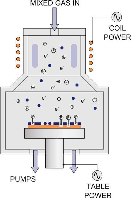
The two technologies used to achieve deep etches in the fabrication of micro-electro-mechanical systems (MEMS) are the Bosch™ and the cryogenic processes. System and process development over many years has allowed the techniques to advance but the fundamental aspects of each remain the same:
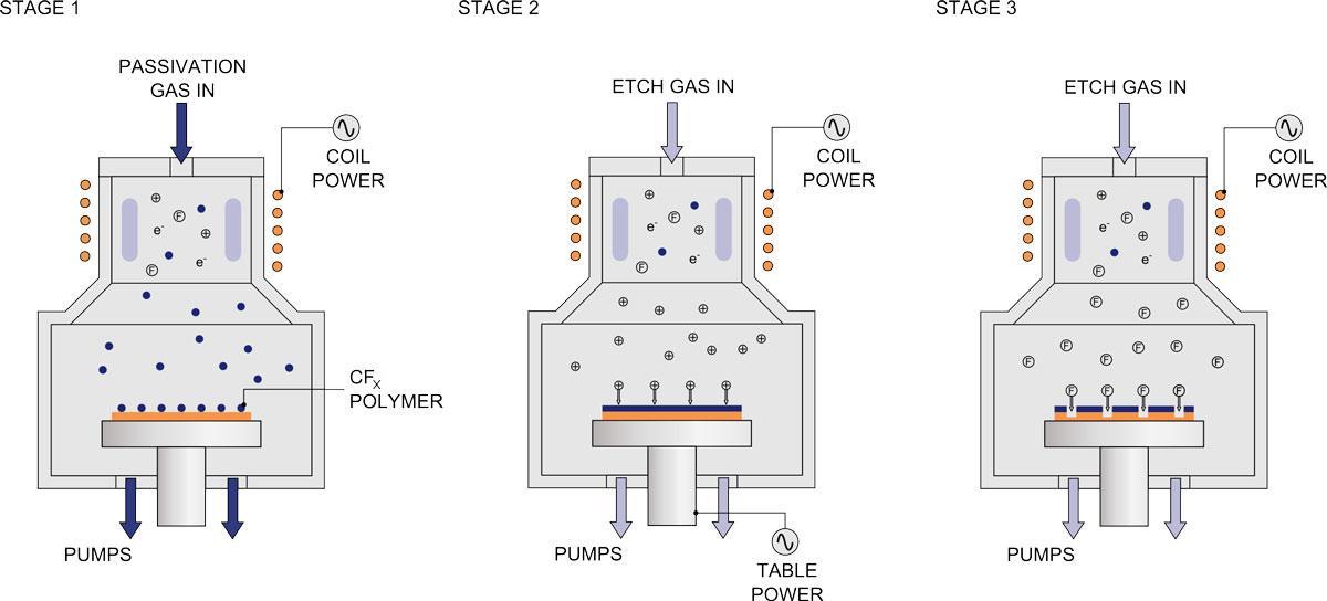
The Bosch™ process uses a fluorine based plasma chemistry to etch the silicon, combined with a fluorocarbon plasma process to provide sidewall passivation and improved selectivity to etch mask. A complete etch process cycles between etch and deposition steps many times to achieve deep, vertical etch profiles. It relies on the source gases being broken down in a high-density plasma region before reaching the wafer.
This technique cannot be performed in reactive ion etch systems (RIE), as these have the wrong balance of ions to free radical species. This balance can be achieved in high-density plasma systems (HDP). The most widely used form of HDP uses inductive coupling to generate the high-density plasma region so is known as inductively coupled plasma (ICP).
High rate, controlled scallops e.g. microfluidics (200 µm depth), vias (> 400 µm depth)
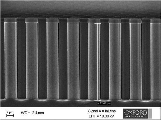
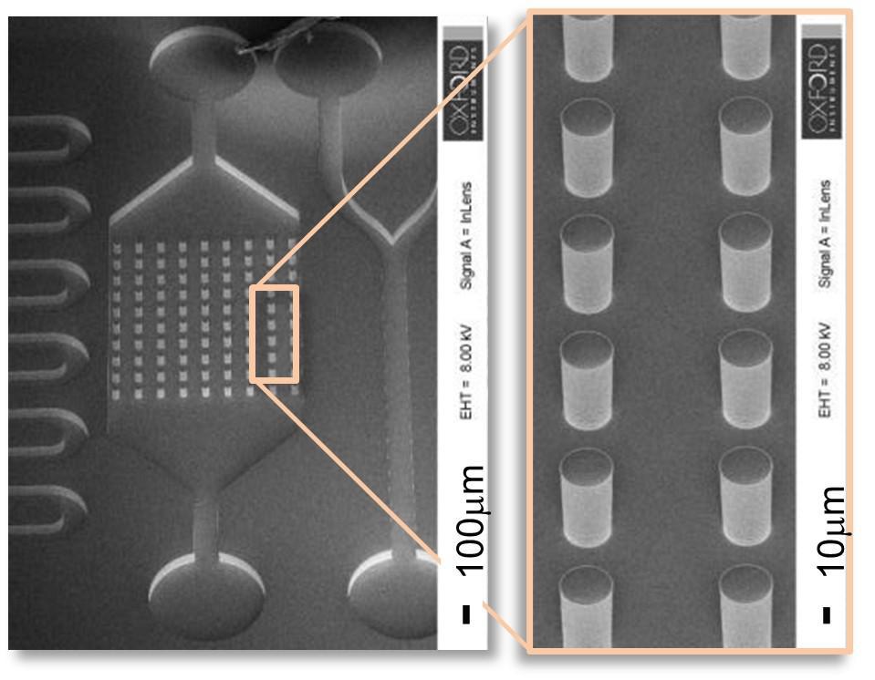
Microneedles created using the Bosch™ process
Just as for the Bosch™ process, this technique also uses SF6 to provide fluorine radicals for silicon etching. The silicon is removed in the form of SiF4, which is volatile.
The main difference is in the mechanism of sidewall passivation and mask protection. Rather than using a fluorocarbon polymer, this process relies on forming a blocking layer of oxide/fluoride (SiOxFy) on the sidewalls (around 10-20 nm thick), this forms at the cryogenic temperatures used and the layer inhibits the attack on the underlying Si layer by the fluorine radicals.
The low temperature and low bias operation also assists in reducing the etch rate of the mask material, which is normally either photoresist or silicon dioxide.
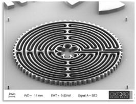
Micro-mould created using the cryo process
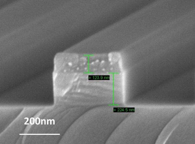
Si waveguide etch
Smooth sidewall cryogenic DRIE (no scallops).
Courtesy TU Twente
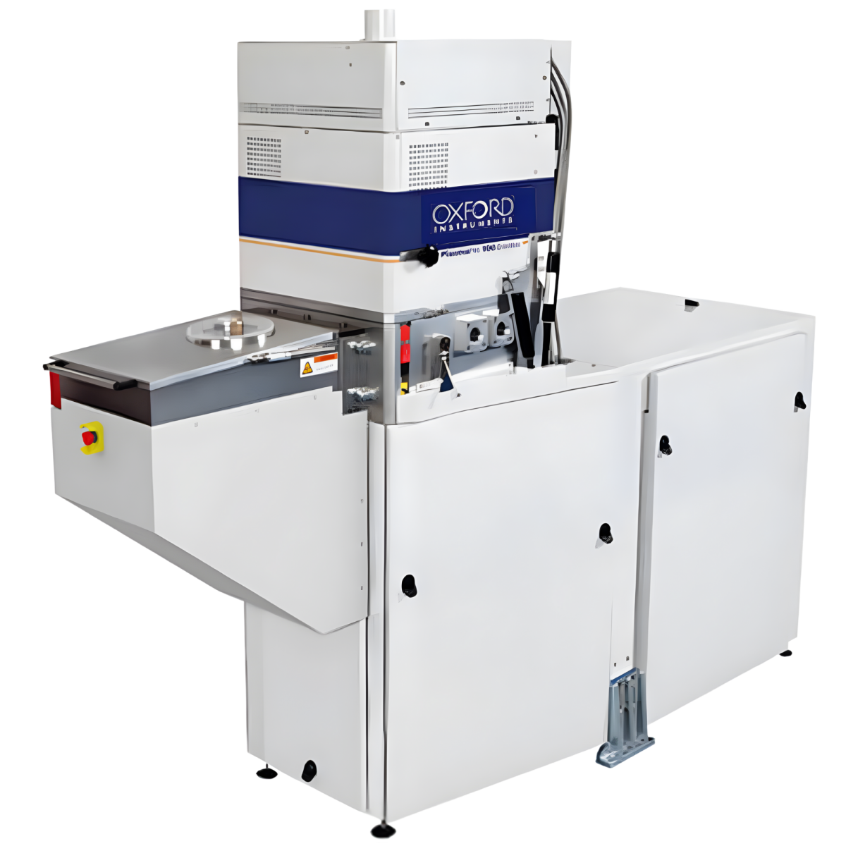
The PlasmaPro 100 Estrelas platform is designed to give total flexibility for DRIE applications - serving a diverse set of process requirements across the MEMS, advanced packaging and nanotechnology markets. Developed for research and volume production, the PlasmaPro 100 Estrelas offers the ultimate flexibility with Bosch™ and cryogenic processes.
DRIE or DSiE combines isotropic silicon etching and passivation steps repeatedly to obtain anisotropic profiles. Using high density plasma source and fast gas-switching capability, this technique enables you to achieve profile verticality, smooth sidewalls and high etching rates with high selectivity to masking materials.
From smooth sidewall processes to high rate cavity etches and high aspect ratio processes to tapered via etches, the PlasmaPro 100 Estrelas has been designed to ensure that the wide range of applications in MEMS, advanced packaging and nanotechnology can be realised without the need to change chamber hardware.
Nano and microstructures can be realised as the hardware has been designed with the ability to run Bosch™ and cryo etch technologies in the same chamber.
Cryo-DSiE is typically used for smooth sidewalls and/or nano-etching and temperature sensitive materials, as it provides low temperature process (» -110 °C)
Parameter |
Bosch™ |
Cryogenic |
Mixed gas |
Rate (μm/min) |
High |
Moderate |
Low |
Selectivity to PR |
Very high |
High |
Low |
Profile |
Vertical |
Vertical or sloped |
Vertical or sloped |
Aspect ratio |
Very high |
High |
Low |
Sidewalls |
Scallops |
Smooth |
Smooth |
ARDE control |
Yes |
Limited |
Limited |
Cleaning |
Regular |
Rare |
Regular |
Min. feature /nm |
≈ 300 |
≈ 10 |
30 |
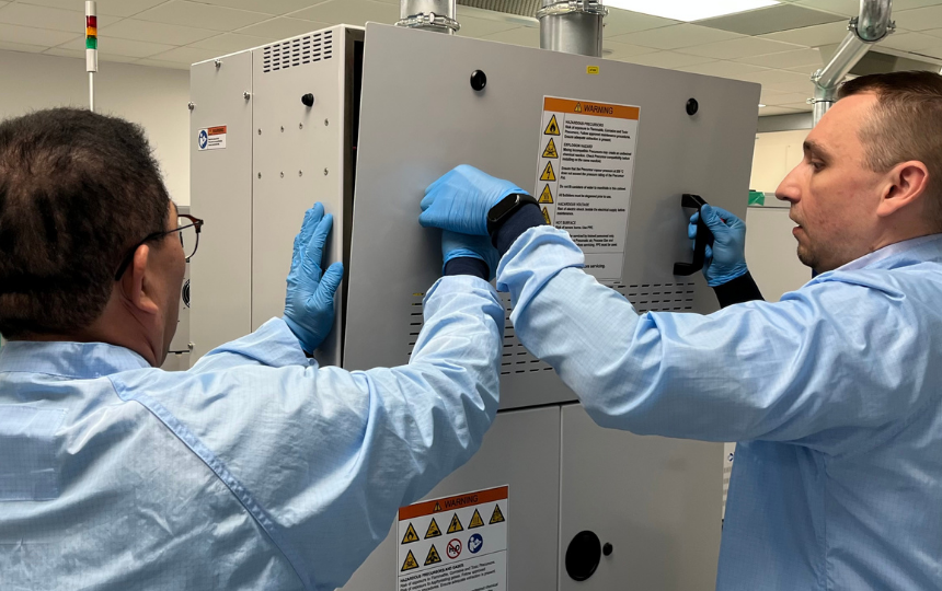
Oxford Instruments is committed to providing a comprehensive, flexible and reliable global customer support. We offer excellent quality service throughout the life of your system.
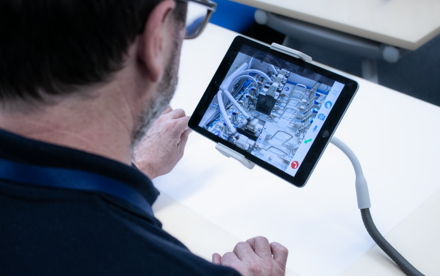
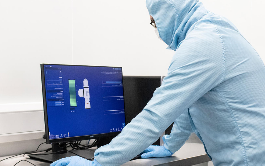
PTIQ is the latest intelligent software solution for PlasmaPro and Ionfab processing equipment.
At Oxford Instruments Plasma Technology, we offer a wide range of technical training courses designed to suit all skill levels and needs.

© Oxford Instruments 2026