Part of the Oxford Instruments Group
Expand
Collapse
Part of the Oxford Instruments Group
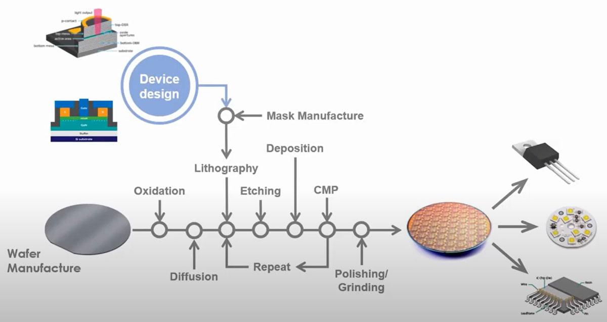
Semiconductor fabrication is a complicated process which requires precise control and analysis to maximise device performance. Here in Oxford Instrument, we work across multiple business units to offer solutions in semiconductor fabrications, characterization, and failure analysis.
This webinar will show how we can help you manufacture high quality semiconductor devices using etch and deposition techniques. We will then explore innovative imaging and analysis techniques to understand and confirm that the device contains the desired properties. Finally, we will cover techniques used to identify device defects and analyse device failures.
The webinar includes the following key learning points:
In this talk, we'll review conventional plasma-based manufacturing methods and provide the context for how they must evolve to be able to support semiconductor development at the nanoscale and beyond. We will look at how these techniques have changed to meet the needs of modern semiconductor manufacturing technology and ask the question, “what next?”.
Energy Dispersive Spectroscopy (EDS) of x-rays and Electron Backscatter Diffraction (EBSD) in the SEM are indispensable analytical techniques, providing quantitative chemical and structural analyses down to a nanometre scale, combined with the imaging capabilities of the electron microscope.
This talk will introduce the theory, the detectors and the applications relevant to the different steps of the semiconductor production process.
Continuous downscaling of semiconductor technology nodes impose ever more stringent requirements on metrology and failure analysis tools.
In this talk, we will cover how atomic force microscopes (AFMs) can be used in process control, defects identification, and in the R&D of new materials. We will demonstrate how AFMs’ unmatched sub-nanometer resolution and wide variety of electrical measurement modes make it an essential characterization tool in present and future devices.

Geoff is a plasma physicist by training; a scientist, an engineer and technologist during the day but, at heart, he is an inventor and an innovator. His career began at Oxford University studying plasma technology for pollution control, then AWE Aldermaston and high energy pulse-power physics and engineering, finally arriving at OI Plasma Technology around the turn of the century to develop plasma systems for the modification and manipulation of materials and surfaces at the nanoscale.
In recent years, he has been developing his Innovation team at Plasma Technology to support current products and develop the products yet to come.

Keith has worked in materials characterization his entire career, first working at Fulmer Research Institute in 1973 as a Research Technician and then later at British Leyland as their metallurgist.
In 1978 he joined the Experimental Techniques Centre of Brunel University as a researcher working with SEM & TEM, EDS, WDS and light microscopy whilst studying for an MSc in metallurgy. He took that experience to GEC Hirst Research Centre in ’84 and led the Applied Electron Optics Group, principally characterizing semiconductor devices and optimizing manufacturing processes.
In 1994, he joined Oxford Instruments Analytical, and have specialised in EBSD, both in product management and applications.

Dr Ted Limpoco is an Applications Scientist at Oxford Instruments Asylum Research. He has over 10 years of AFM experience in nanoelectrical, nanomechanical, and nanotribology techniques.
He was previously a postdoctoral fellow at the University of Illinois at Urbana-Champaign and has a PhD in chemistry from the University of Florida.
© Oxford Instruments 2024