Part of the Oxford Instruments Group
Expand

Inductively Coupled Plasma Etching (ICP RIE)

ICP RIE etching is an advanced technique designed to deliver high etch rates, high selectivity and low damage processing. Excellent profile control is also provided as the plasma can be maintained at low pressures.

The Cobra® ICP sources produce a uniform, high density plasma with the capability to operate at low pressures. Substrate DC bias is independently controlled by a seperate RF generator, allowing control of ion energy giving excellent results tailored to specific process requirements.
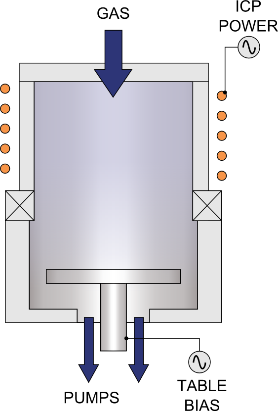

Diagram of ICP etching system technology

Key Benefits

  • Unique wide temperature range electrode from -150ºC to +400ºC, range of process solutions across an extensive variety of materials and devices
  • High etch rates achieved by high ion density (>1011 cm3) and high radical density
  • Source designed for excellent cross wafer uniformity
  • Control over selectivity and damage achieved by low ion energy
  • Excellent profile control with high density of reactive species at low pressure processing
  • Independent control of the ion energy through separate substrate DC bias control
Request More Information

Hardware


PlasmaPro 80  
PlasmaPro 100  PlasmaPro Polaris
Electrode size 240mm
Loading Open load
Load lock or Cassette
Wafer size Up to 50mm (2")* Up to 200mm Up to 200mm
MFC controlled gas lines 8 or 12 line gas box available 3-5 close coupled gas lines with options for 8-12 external 8 or 12 line gas box available
Wafer stage temperature range -150 to 400ºC
Request Quote for ICP RIE Systems

Applications

  • GaN etch for LEDs or lasers and power devices
  • Vertical Indium Phosphide (InP) waveguides with smooth etch surfaces
  • Non-selective GaAs/AlGaAs, achieving smooth sidewalls for VCSEL
  • Precise VCSEL mesa etching with excellent etch depth control
  • Highly selective GaAs/AlGaAs for optoelectronics
  • Oxide etching for waveguides
  • Failure Analysis Applications, removing:
    • isotropic polyimide and isotropic nitride (passivation),
    • anisotropic Oxide (IMD/ILD)
    • Low-K Oxide
    • Al and Cu
    • Backside Bulk Si

Features

  • Separate RF and ICP generators provide separate control over ion energy and ion density, enabling high process flexibility
  • Chemical and ion-induced etching
  • Can also be run in RIE mode for certain low etch rate applications
  • Can be used for deposition in ICP-CVD mode
  • High conductance pumping port provides high gas throughput for fastest etch rates
  • Electrostatic shield eliminates capacitive coupling, reduces electrical damage to devices, reduces chamber particles
  • Wafer clamping and helium cooling as standard, providing excellent temperature control with the option of a wide temperature range

ICP Etching of a InP with smooth sidewalls and clean surface

ICP Etching of a InP showing smooth sidewalls and clean etched surface
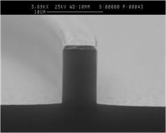
ICP Etching of SiO2 waveguide using a Cr mask

ICP Etching of SiO2 waveguide using a Cr mask

ICP Etching Systems

PlasmaPro 80 ICP
PlasmaPro 100 Cobra ICP
PlasmaPro 100 Polaris ICP

PlasmaPro 80

  • Excellent wafer temperature uniformity
  • Accommodates wafers up to 200mm
  • Optimised electrode cooling

PlasmaPro 100 Cobra

  • High density of reactive species
  • Wide temperature range electrode, -150°C to 400°C
  • Applied to a wide range of markets

PlasmaPro 100 Polaris

  • High throughput with superb etch results
  • High density plasma etch source
  • Enhanced ion control and uniformity
Download PlasmaPro 80 Brochure
Download PlasmaPro 100 Brochure
Download Polaris Brochure

Related Content