 Part of the Oxford Instruments Group
Expand
Collapse
15 Apr 2019 | Author: Mark Dineen
You say ‘diamond’ and it gets the imagination going: glamour, wealth and exclusivity the material has had some of the best marketing in history! As well as being a very popular gemstone, it has some amazing electrical and physical properties. This has been known for a long time, however, it is only recently that the technology to take advantage of these properties is becoming more mature.
Diamond and its applications, other than looking good, was discussed in depth at the very first, and very good, Diamond Day recently held in Bristol.
One of the most interesting items that came out of the meeting was the consideration of the effect of heat in a satellite system, A. Barnes from the European Space Agency (ESA) and Daniel Francis of Akash Systems discussed how diamond and wide bandgap devices can really improve performance in what is a very harsh environment. A satellite has many electronics and mechanical parts, each one of these is not 100% efficient and each will generate some heat, Avaram Bar-Cohen of Raytheon showed data that the hotspots on a high power amplifier exceeds that of the surface of the Sun! So where does the heat go? The satellite is in space so conduction away from the satellite is non-existent, radiation is possible but again is pretty poor. So, heat is generated and stays for a lot longer than a system down at sea level…which means you should a) try to generate as little heat as possible b) move the heat away from sensitive areas as quickly as possible and have active cooling within the satellite.
The more efficient electronics comes in the form of wide band gap materials, GaN and SiC, used for the power electronics. While getting the heat away from sensitive areas is much improved using diamond as it has a thermal conductivity of 2000 W/mK, compared to Si for example whose thermal conductivity is 148 W/mK, this means it is far far better at moving heat from one area to another.
The main obstacle has been, and remains to a great degree, is how on earth do you get the diamond onto the other material. If you glue it the interface can act as a thermal barrier so reduces the benefit. Growing it would be best of all but it is grown at very high temperatures to get good quality material and does not grow naturally on many materials. Oliver Williams from the Cardiff University based Cardiff Diamond Foundry presented slides on how you can improve it’s adhesion on GaN by using an AlN seed layer. This has enabled them to grow 100µm of diamond on AlN/GaN. With this thickness you can start doing interesting things with cooling channels through the diamond, so the heat is conducted from the active area of the device and the coolant transfers the heat away from the package. Meaning the device can be pushed harder and the temperature remains stable.

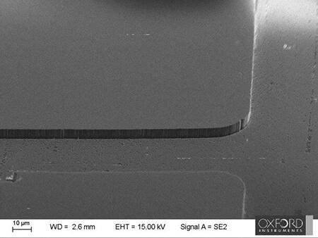
Figure 1: Deep diamond feature etched using Inductively Couple Plasma – Reactive Ion Etch (ICP-RIE).
Diamond may be incredibly difficult to grow but when grown properly it is extremely hard. This in turn makes it difficult to create features in it as it is so resilient. Here at Oxford Instruments Plasma Technology we have been working on etching diamond for a long time. First etching it to form ultra-sharp miniature scalpels for eye surgery and more recently we have worked on etching features into diamond films.
So, diamond is a tricky material to process and use, but its properties are so special for some applications it is worth all the effort. I look forward to the next Diamond Day!
For more information contact us at plasma-experts@oxinst.com or use the button below.