Part of the Oxford Instruments Group
Expand
Collapse
Part of the Oxford Instruments Group
I was at a conference a few years back where the VCSEL industry was described as forever being a ‘cottage industry’, for those not familiar with the term this means small scale with individual products made to specification. Fast forward to 2017 with Apple introducing Face ID on it’s iPhone X and this comment is blown away. The market pull from millions of iPhones means that millions of identical VCSELs need to be produced at an effective cost, VCSELs have gone from cottage industry to high volume manufacturing. What has this meant for VCSEL manufacturing and what will it mean as new applications, LiDAR etc come into play?
One of the maxims of the semiconductor industry is that the bigger the wafer size the better, VCSEL wafers are no exception. The recent developments have taken wafers from 100mm to 150mm which offer more mm2 per process run for a similar cost. However, increased surface area can have a negative effect on yield which is where we go next.
The VCSEL manufacturing process has been plagued with low yield for a long time. Take for example the oxidation of the aperture. The oxidation rate varies exponentially with the Al content of the layer. So if the Al content varies even slightly across the wafer you will get a large variation in aperture size and therefore performance across the wafer and your yield will be poor. There have been great strides in epi layer control and also oxidation rates in order to reduce this effect. It has been proven successful at 150mm.
Plasma processing, which is where Oxford Instruments Plasma Technology comes in, has also had to develop solutions. Etching complex multi layers of different materials, smoothly and consistently across the wafer is not trivial. We have developed process and hardware solutions specifically for this task and are very excited to see our high volume manufacturing customers use these with great results.
Yield speaks to cost of ownership which leads to company profitability so it is something that is always on our minds asking ‘What’s next?’
The drive to higher powers, getting more light out for a given surface area. Achieving this means clustering the VCSELs closer together, so how does this effect the plasma processing? Looking at something in a simple, physical (I like simple) way you don’t want the geometry of one device to overlap with another. If you do, then interference can happen and devices run less efficiently. In real terms this means sharper features, no long ‘foot’ at the bottom of one VCSEL merging into the ones next door. We have developed a superb low foot etch process which means VCSELs can be made closer together than ever before.
Another example of different requirements is for the passivation of the surface. As VCSELs get closer the gap between them closes relative to the height of the feature and this can lead to aspect ratio (AR) related effects whereby plasma processes are material transport limited. By using sophisticated techniques such atomic layer etching (ALD) the AR effect can be eliminated at these levels ensuring a conformal coating of material across the whole surface.
VCSELs have entered the mainstream of consumer devices proving highly successful in delivering new user experiences. The future will see them being even more widely adopted and Oxford Instruments Plasma Technology as the choice for Compound Semiconductor high volume manufacturing is enabling the cost of ownership to make this happen.
Learn how to produce high power VCSEL arrays here.
Dr Mark Dineen
Technical Marketing Manager, Oxford Instruments Plasma Technology


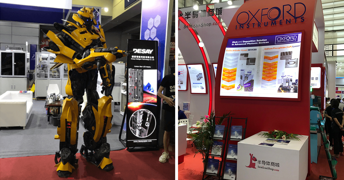
China International Optoelectronics Expo 2019
2019
2018

© Oxford Instruments 2026