 Part of the Oxford Instruments Group
Expand
Collapse
Part of the Oxford Instruments Group
Fitting to the contents of this post on collaboration, this post will appear both on Atomic Limits and on the Oxford Instruments Plasma Technology blog. What defines a truly successful collaboration? It has to be something where the whole is greater than the sum. With the partnership between Oxford Instruments Plasma Technology and Eindhoven University of Technology now entering its 13th year this is a great example of how manufacturing can get really close to, and benefit from, the research at a leading university.
The Oxford Instruments’ motto “The Business of Science” is very true in my case. Besides my role as atomic scale segment specialist for Oxford Instruments Plasma Technology, I work one day a week for the Eindhoven University of Technology as a part-time assistant professor in the group of Erwin Kessels. I work on atomic layer deposition (ALD) and its application where the main focus is on understanding, controlling and using surface and plasma processes.
I enjoy the science and being part of academia and furthermore I am in an ideal position to support the strong collaboration between the research group and Oxford Instruments. This is a collaboration which has been going strong since 2005, it has produced many positive fruits for both sides. On certain subjects the collaboration is very direct and there is a lot of interaction. Examples of this are the development of substrate biasing on our FlexAL system and the introduction of the FlexAL2D system for the growth of 2D materials.
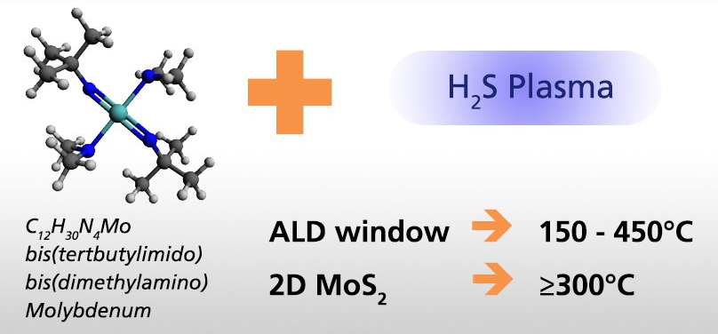
The FlexAL2D configuration developed at Oxford Instruments and first installed at Eindhoven University of Technology allows low temperature growth of 2D MoS2 and a wide ALD window. The work is the first stepping stone to a whole set of 2D sulfide film growth studies by ALD.
In other cases, for development of a new ALD process for instance, I would often be only slightly involved, where I would advise on process conditions, potential solutions to problems or interpretation of results. This close working has strong benefits for Oxford Instruments as it provides direct feedback on how the plasma equipment impacts device performance. This is key to our business: understanding deeply how the plasma affects the device enables Oxford Instruments to deliver solutions to their customers that give them the best devices. It is that simple. Eindhoven University of Technology gains by having a plasma and ALD specialist on site who is also part of industry. The back and forth of ideas and knowledge increases the pace of research and sometimes brings new ideas on where it should go.
One idea which has been developing in the field which has been specifically prominent at both Oxford Instruments and Eindhoven University of Technology is the idea of Atomic Scale Processing or Atomic Layer Processing. The grouping of ALD and ALE is very natural as both are cyclical and deal with self-limiting nanolayer control, but there is also synergy with 2D material growth and surface cleaning or treatment since also there understanding of surface processes and control thereof are essential. Furthermore for all these techniques there is the goal to make nanometer control easy to do at wafer scale. Therefore all these techniques can be grouped together. Oxford Instruments generally labels these as Atomic Scale Processing where ALD, ALE and 2D material growth are the main focus and tools dedicated to these techniques can for instance be easily clustered together to process without vacuum break.

Oxford Instruments has put strong emphasis on their atomic scale processing capability where it highlights that ALD, ALE and 2D materials growth can be combined. This could be of interest for a wide range of devices and opens up new application possibilities.
28 Feb 2019 | Author: Dr Harm Knoops
Eindhoven University of Technology has included also Atomic Layer Cleaning (ALC) and has grouped 2D materials work under ALD and leave out CVD and PECVD methods thereof. In principle the exact grouping and naming are not essential. What is important is the notion that combining or grouping such techniques can have new benefits and that knowledge from these techniques and fields can be combined to provide new insight and possibilities.

Atomic layer processing or atomic scale processing can mean many things. In this updated illustration by Eindhoven University of Technology, deposition, etching and cleaning are indicated together with respective active areas of research and some key applications.
One of my general tasks which is beneficial for both the university and Oxford Instruments is highlighting the work utilizing FlexAL and OpAL ALD systems. Below a list of papers from 2018:
This list highlights the diverse nature of the work done in the Eindhoven group and several topics can be identified. Besides topics such as substrate biasing, perovskite solar cells, and 2D materials, you’ll notice that there are quite some papers related to thin films for crystalline Si solar cells and this remains an active research topic in the group. Interesting to see how novel materials and interface layers such as Nb2O5 and POx show excellent properties for passivation and potentially also in stacks for new types of contacts. Most of the works relate to ALD, but one paper related to isotropic plasma ALE, an indication that the era of atomic scale processing has been entered. Of course there are many upcoming works and I am very curious how the different subjects will develop over the coming years. I would say keep an eye on the publications of our users and the work from Oxford Instruments.
Successful collaborations require people and organisations that are pulling in the same direction. Oxford Instruments is sticking close to this customer and through the collaboration they are pushing plasma ALD solutions to solve more and more problems – a successful collaboration indeed.
For more information on Oxford Instruments Plasma Technology applications visit our page or drop us a line through our email Plasma-experts@oxinst.com
Ask us a question!
© Oxford Instruments 2026

