Part of the Oxford Instruments Group
Expand
Collapse
Part of the Oxford Instruments Group
13 June 2019 | Author: Dr Harm Knoops
Gallium Nitride (GaN) is a wonderful material for power electronics due to its wide band gap. With the electrification of transport, GaN power devices are becoming more and more important and device cost and efficiencies are critical. For many applications E-mode or normally-off devices are important for fail-safe requirements and gate dielectric layers (such as Al2O3) are vital to obtain more efficient devices in E-mode configurations.
Read below the 5 ways in which Atomic Layer Deposition (ALD) can help to achieve these goals and benefit GaN devices:
The thin-film gate dielectric for GaN-based transistors has to be of high quality to result in low leakage and high breakdown voltage. The benefit of ALD and particularly of plasma ALD is that it deposits dense layers resulting in a superior performing device.
Breakdown doesn’t occur until a high voltage which is due to the high quality of the layer and the low level of pin-holes resulting from ALD’s ability to fill voids. Interestingly these properties are obtained at modest temperatures of 200 to 400°C avoiding high temperatures needed for some other techniques.
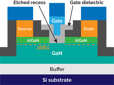
Figure 1: Cross-sectional schematic of normally-off GaN-on-silicon power device with etched recess and conformal gate dielectric.
Recess structures can be challenging for many directional deposition techniques such as sputtering. The recess geometries used in GaN devices have relatively modest aspect ratios and are quite easy for most ALD processes.
Due to the self-limiting nature of ALD these can be coated conformally with equal thickness throughout the structure. Generally no change in process recipe is needed to maintain conformal deposition for a wide range of device structures and associated aspect ratios.
Both in production and research, thickness and property control are essential. The self-limiting nature of ALD allows for excellent uniformity over large areas, making all devices perform the same. Since the resulting film thickness is based on the number of ALD cycles chosen, excellent reproducibility is obtained as well. Thereby providing the same thickness each run and little variation from machine to machine or day to day.
Due to the stepwise nature of ALD it is also relatively easy to modify the recipe or mix materials together. This property of ALD makes it easy to follow a future roadmap of material modification and process improvement. For instance by going to higher-k materials such as HfO2 or going to nitride dielectrics such as AlN.
In comparison to other semiconductors, the GaN surface is one of the most process-sensitive in the electronics industry. Luckily, remote plasma ALD processes are low damage to GaN. Optimizing the process conditions and limiting ion energy and flux allows for low defect densities the interface and in the film. At the same time reactive species densities and fluxes are sufficient to grow high-quality material and have acceptable throughput of the process.
After the preceding processing step or after air exposure the GaN surface can have a low-quality surface oxide and can contain defects and impurities such as carbon. Both remote plasma pulses and ALD precursor pulses can be used to reduce these. Trimethylaluminium (TMA) is a common ALD precursor for dielectric Al2O3 growth.
Interestingly, TMA can actually be used as reducing agent to remove some of the surface oxide of GaN. Hydrogen and nitrogen plasmas are known to be able to reduce surface oxides as well and are known to be able to remove impurities such as carbon.
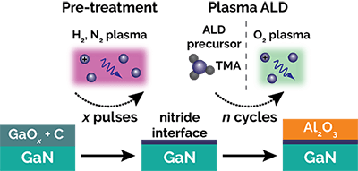
Figure 2: Example of H2 or N2 plasma pre-treatment and Al2O3 plasma ALD on GaN to illustrate the effect of pre-treatment and ALD on the surface composition and structure.
We expect that these 5 ways are just the tip of the iceberg in terms of the possibilities that ALD provide for power semiconductors. Combining the pre-treatments and plasma ALD with subsequent processing such as anneals is expected to allow for even further optimised device performance. Let us know your questions and ideas in the comments below!

Dr Harm Knoops
Atomic Scale Segment Specialist, Oxford Instruments Plasma Technology


© Oxford Instruments 2026