 Part of the Oxford Instruments Group
Expand
Collapse
Part of the Oxford Instruments Group
Endpoint Detectors (EPD) are an important tool for achieving optimal process results. The use of an EPD ensures processes are carefully controlled and consistent, to ensure reliable repeatable results are achieved wafer-to-wafer and batch-to-batch. Several techniques exist and it is vitally important to understand the strengths of each and how they fit with your process requirements to achieve what you need.
We offer EPD upgrades under these two categories:

|
|
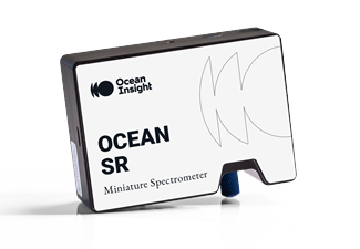 Ocean Optics SR4 Spectrometer
|
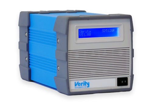 Optical Endpoint Verity SD 1024GH
|
Optical Endpoint Verity SD 1024G
|
| Options | Ocean Optics SR4 Spectrometer | Verity SD 1024GH | Verity SD 1024G |
| Wavelength range | 190 - 900 nm (configurations available within this range) | 200 - 800 nm | 200 - 800 nm |
| Spectrometer | Real time | Real time | Real time |
| Endpoint | Yes | Advanced algorithms | Advanced algorithms |
| Chamber condition analysis | Yes | Yes | Yes |
| Etch process monitor | Yes | Yes | Yes |
| Reprocess | No | Yes | Yes |
| Resolution | Good for general single layer process | Superior for complex multilayer | Excellent for complex multilayer |
| Suitable for | PECVD, RIE, ICP-RIE, and CVD systems | RIE and ICP-RIE Systems | RIE and ICP-RIE Systems |
| Example Applications | PECVD chamber clean, SiO2/SiNx etch, PR strip, general purpose etching | SiO2/SiNx etch, GaAs/ AlGaAs/ GaSb/ AlGaSb, InP/ InGaAs/ InGaAsP/ InAlGaAs, Metals, Plasma analysis, Deep Si, GaAs VCSEL | SiO2/SiNx etch, GaAs/ AlGaAs/ GaSb/ AlGaSb, InP/ InGaAs/ InGaAsP/ InAlGaAs, Metals, Plasma analysis |
Optical emission spectroscopy (OES) monitors the light emitted by the plasma. Measuring the intensity of light emitted at a specific wavelength in a spectrum allows a relative measurement of the concentration of a given species.
Etch by-products and gas species have characteristic emission wavelengths, so process endpoints can be detected by looking for changes in these emissions as the etch reaches a new layer. OES end pointing typically requires an etched area of several cm2 to provide a detectable concentration of etched species in the plasma, depending also on etch rate and plasma emission intensity.
A popular application of OES is in the plasma cleaning of PECVD chambers, but the same principle is also used for etch chambers. In PECVD for example, measurement of the fluorine emission intensity is used to determine the endpoint of chamber plasma cleaning. During cleaning the fluorine concentration will be low as it is being consumed by the etching process, but it will rise sharply when the chamber walls become clean, providing an endpoint.
| Upgrade | Available on |
| Ocean Optics SR4 Spectrometer | Any platform operating with PTIQ software |
| Verity SD1024G Spectograph | PlasmaPro 100, PlasmaLab 100, PlasmaLab 133 |
| Verity SD1024GH Spectograph (High Performance) | PlasmaPro 100, Estrelas, PlasmaLab 100, PlasmaLab 133 |
| Verity PM140 Detector 704 nm | PlasmaPro 80, PlasmaPro 800 |
Most endpoint detection upgrade installations are typically completed within two days, including travel and introductory training on operating an endpoint detector.
For pricing, a free consultation, and more information on optical end point detectors, please contact your local customer service sales team.
 Horiba LEM
|
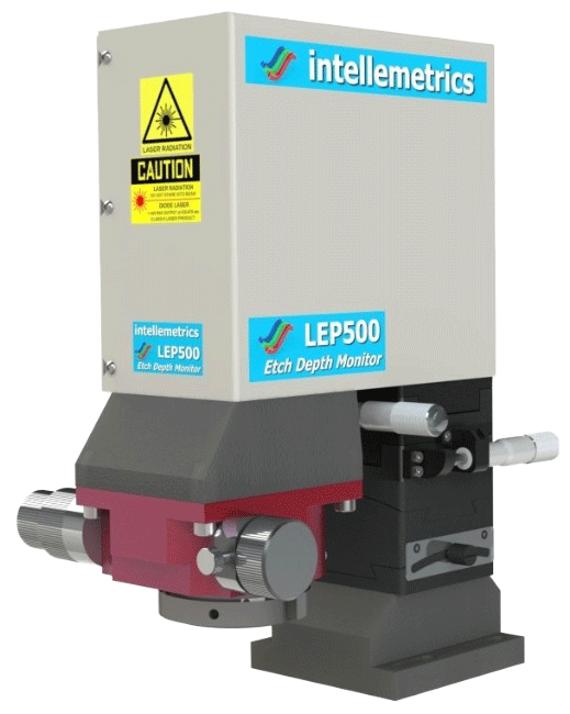 Intellemetrics LEP500
| |||
| Options | Laser Endpoint Horiba 670nm | Laser Endpoint Horiba 905nm | Laser Endpoint Intellemetrics LEP500 670nm | Laser Endpoint Intellemetrics LEP500 980nm |
| Movement | XY and tilt adjustment | XY and tilt adjustment | ||
| Sample image magnification | x50 | x50 | ||
| Laser wavelength | 670/ 905 nm | 670/ 980 nm | ||
| Laser spot size | 30 to 60μm | Working Distance dependant. 8 to 40μm at FWHM | ||
| Layer structure modelling | No | Yes | ||
| Suitable for | RIE and ICP-RIE Systems | RIE and ICP-RIE Systems | ||
| Example Applications | SiO2/ SiNx, Metals, GaAs/ AlGaAs/ GaSb/ AlGaSb, PR strip, Failure Analysis | Metals, GaAs VCSEL, GaAs/ AlGaAs/ GaSb/ AlGaSb, InP/ InGaAs/ InGaAsP/ InAlGaAs, PR strip | ||
| Optional | Motorised "XY" table for laser interferometer is available as optional extra with these two upgrades. The Motorised ""XY"" stage option allows the laser endpoint beam to be positioned accurately via a user joystick control. | - | ||
A laser interferometer measures the change in reflectance of the wafer surface during etching or deposition, by focussing a laser spot onto the wafer and measuring the intensity of the reflected laser light. The laser interferometer camera also provides a TV image of the wafer surface to allow precise positioning of the laser spot onto the correct region.
The etch rate can be calculated by monitoring ripples in the laser signal due to interference effects within the thin film, allowing the etch to be stopped at a certain depth within the layer. Interfaces between layers can also be detected, as this typically results in an abrupt change in reflectance.
Laser interferometry typically requires user intervention to position the spot before each run (unless a specific region of the wafer is dedicated for laser endpointing).

| Upgrade | Available on |
| Horiba 670nm | PlasmaPro 100, PlasmaPro 80 |
| Intellemetrics 670nm | PlasmaPro 100 |
| Intellemetrics 980nm | PlasmaPro 100 |
Most endpoint detection upgrade installations are typically completed within two days, including travel and introductory training on operating an endpoint detector.
For pricing, a free consultation, and more information on laser end point detectors, please contact your local customer service sales team.

© Oxford Instruments 2026

