 Part of the Oxford Instruments Group
Expand
Collapse
4 June 2020
Experiencing fully immersive augmented reality requires a major leap in several technologies. From 5G to microdisplays, nanofabrication is at the heart of this challenge.
In addition, AR headsets need to combine the largest amount of high-end technology at the smallest form factor.
To make a headset, you need:
And that's just to name a few!

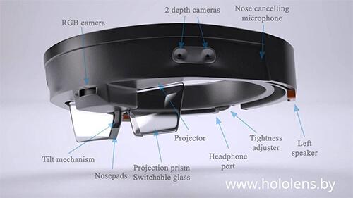
Microsoft Hololens headset
Amongst these many technical challenges, one key challenge is to produce a virtual image bright enough that it comfortably blends with the real-world indoor and outdoor.
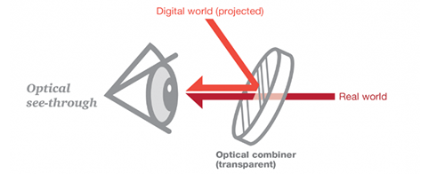
To do so, combiners are used to “combine” a virtual image to the real world. A virtual image is projected to the user’s eye whilst transmitting a real image.

Optical combiner technology. Credit: PwC
Of the numerous technologies developed for combiners, the optical waveguide approach is a promising technology. Waveguide combiners can achieve high field-of-view at low form factor. How seamless the virtual image appears will then partly result from the display brightness in Nit, the efficiency of the combiner and the lens transparency.
In diffractive waveguide based on surface relief grating (SRG), the incident light waves flow into the waveguide at an angle set by the first grating, in-coupler. This angle is set to allow for Total Internal Reflection through the waveguide and the light is finally extracted to exit into the pupil via a second grating the out-coupler.
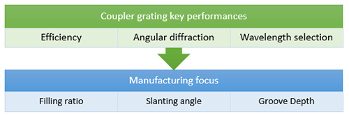
The in- and out-couplers are SRG which are nano metric grooves. The geometry of the structures directly defines the coupling efficiency. More light is collimated into the waveguide when using slanted features which then results in increased efficiency. This is critical to ensure the digital image appear with sufficient definition and brightness to the human eye.

Surface relief gratings are generally replicated from a master mould. Ion beam etching (IBE) is a technique well suited to fabricating the master mould for slanted gratings.
Since the geometry of the structure partly defines the coupling efficiency, precise definition of the dimensions of the master mould is required. However, there are many challenges to producing SRGs on wafer scale with satisfying yield:

Defined SRG on Si master mould

Non-parallel SRG on master mould
If you would like to learn more on processing slanted features, take a look at our AR Solutions.
2020
2019