Part of the Oxford Instruments Group
Expand
Collapse
Part of the Oxford Instruments Group
Atomic Layer Deposition (ALD) is an advanced deposition technique that allows for ultra-thin films of a few nanometres to be deposited in a precisely controlled way. Not only does ALD provide excellent thickness control and uniformity but 3D structures can be covered with a conformal coating for high-aspect-ratio structures.
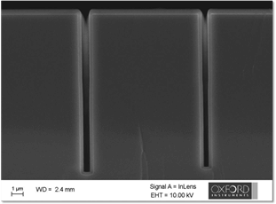
Conformal coating of high aspect ratio (15:1) structure with high-rate plasma ALD SiO2.
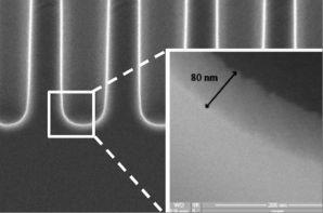
80 nm remote plasma ALD Al2O3 film in 2.5 mm wide trenches with aspect ratio ~10, deposited with FlexAL.
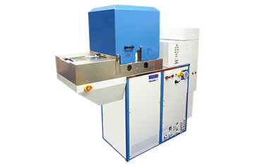
The FlexAL atomic layer deposition (ALD) system offers a broad range of optimised high-quality plasma ALD and thermal ALD processes with maximum flexibility in precursors, processes gases, and hardware configuration within a single process chamber.
RF biased electrode option available for control of film properties
Industry-standard cassette to cassette handling for higher throughput
Maximum flexibility in the choice of precursors, process gases, hardware features and options
Optimised to maintain low-damage, high-quality substrates
Atomic Layer Etching (ALE) is an advanced etch technique that allows for excellent depth control on shallow features. As device feature size reduces further and further ALE is required to achieve the accuracy required for peak performance.

© Oxford Instruments 2026