 Part of the Oxford Instruments Group
Expand
Collapse
Part of the Oxford Instruments Group
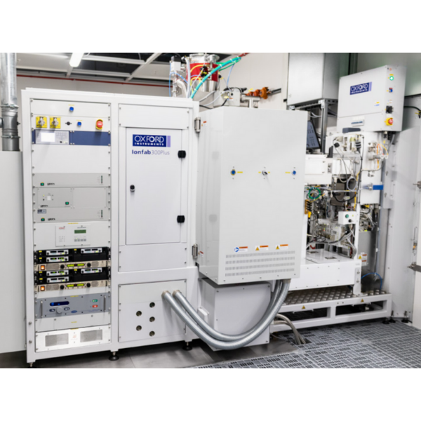
We’re excited to bring you Semi Interface Issue #4: WBG Power Edition, where we explore the transformative potential of silicon carbide (SiC) and gallium nitride (GaN) in reshaping power and RF electronics. This edition brings together insights from leading global experts, showcasing advancements in plasma technologies for interface optimisation and nitride ALD innovations driving volume manufacturing and reliability. We also highlight SiC’s emerging role in augmented reality, enabling immersive user experiences with exceptional clarity, durability and comfort.
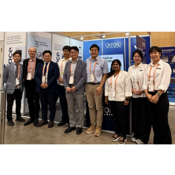
This issue features collaborative innovations, such as the co-development work between the University of Warwick and Oxford Instruments on trench etch & fill, and atomic scale processes presented at ICSCRM 2025 in Busan, South Korea. We also report on Singapore’s advancements, including insights from SEMICON Southeast Asia and Oxford Instruments’ involvement in the Singapore NSTIC GaN initiative. Additionally, expert voices from industry leaders provide perspectives on atomic-scale plasma processing, with a particular focus on South Korea’s developments.
Packed with cutting-edge technology and global perspectives, Semi Interface Issue #4 highlights how SiC and GaN are evolving into strategic technology platforms, transforming industries and enabling the next generation of innovative applications.
Download Magazine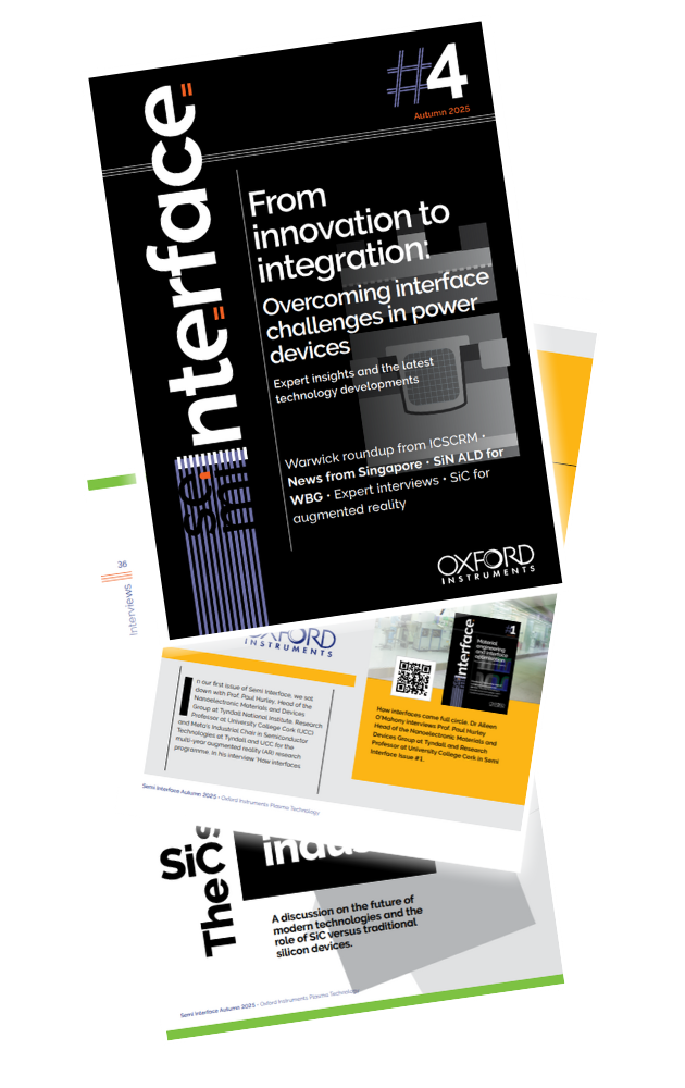
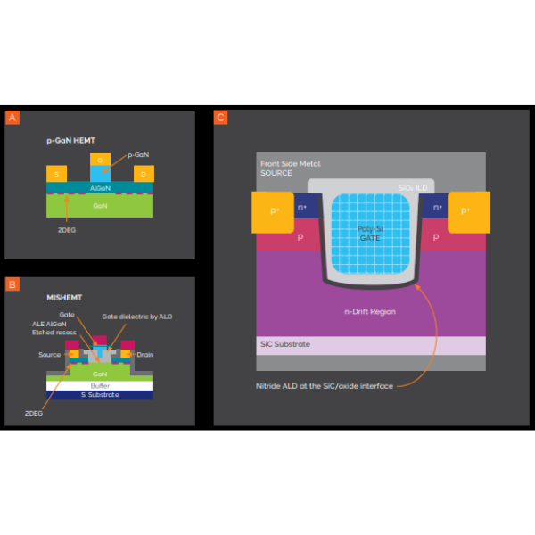
The growing demand for high-efficiency, compact power electronics is driving the adoption of silicon carbide (SiC), a superior wide bandgap semiconductor material ideal for next-generation power devices. Dr Arne Benjamin Renz, Assistant Professor and leading researcher in silicon carbide (SiC) power electronic interfaces at the University of Warwick’s School of Engineering, writes about the university's collaborative research with Oxford Instruments, addressing key challenges in SiC device fabrication and highlighting the work presented at ICSCRM 2025.
'The collaborative research also relies on advanced characterisation tools to evaluate and fine-tune the developed processes'
A panel discussion hosted at the British High Commission in Singapore explored bridging research and industry by integrating quantum technology into the semiconductor sector. Moderated by Ang Wee Seng, the discussion featured Prof. Manas Mukherjee, Bas Derksema, and Dr. Sebastian Woods, focusing on Singapore's vision to become a quantum technology hub through the National Quantum Office (NQO) and its National Quantum Federated Foundry (NQFF) program. The event emphasized collaboration opportunities between the UK and Singapore, with Oxford Instruments highlighting its expertise in supporting quantum innovation and translating research into commercial applications.
'...from basic R&D to targeted process and application development, Plasma Technology is ideally suited to be a partner for entrants embarking on this journey.'
Oxford Instruments is playing a pivotal role in Singapore’s National Semiconductor Technology Innovation Centre (NSTIC) initiative, with a focus on advancing gallium nitride (GaN) and silicon carbide (SiC) semiconductor technologies. Matt Kelly, Managing Director of Oxford Instruments Plasma Technology, explains how the opening of the gallium nitride initiative aims to position Singapore as a global leader in semiconductor innovation, fostering economic growth, job creation, and advancements in sustainability and technology across multiple high-growth industries.
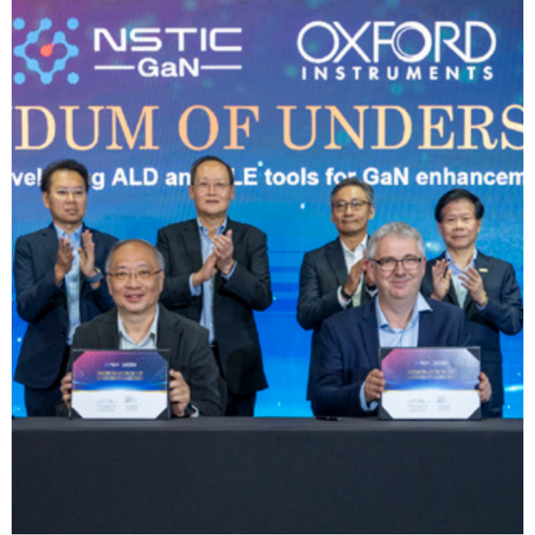
'Our goal in this project is to collaborate closely with A*STAR, local research institutions, and industry players to drive R&D efforts in GaN / SiC technology.'
Wide bandgap (WBG) semiconductors like gallium nitride (GaN) and silicon carbide (SiC) are revolutionising power electronics by delivering unprecedented efficiency, thermal management, and power density, enabling advancements across industries such as renewable energy and electric vehicles. However, challenges like surface states and interface traps limit their potential. Oxford Intruments Plasma Technology's Dr Aileen O'Mahony, Bas Derksema and Grant Baldwin discuss how Plasma Enhanced Atomic Layer Deposition (PEALD) of silicon nitride is emerging as a vital solution to enhance reliability and performance for next-generation devices.
'Wide bandgap semiconductors like GaN and SiC are redefining the boundaries of power electronics'
Dr. Vijay Ramya Kolli, Head of Strategic Production Markets at Oxford Instruments Plasma Technology, joins with Prof. Anant Agarwal, Principal Investigator of the SiC Power Devices Reliability Lab at Ohio State University, to explore the current state and future potential of silicon carbide (SiC) as a next-generation semiconductor material, and the transformative impact SiC could have across many industrial and commercial sectors.
'SiC allows you to move the same amount of power with fewer losses, in a smaller, lighter, and often cooler system.'
Ian Wright, VP of Production Sales at Oxford Instruments Plasma Technology, spoke with Dr. Kolja Haberland, Chief Technology Officer at LayTec, during this year’s CS Mantech conference to discuss LayTec’s expertise in the GaN power electronics (PE) and radio frequency (RF) markets. Dr. Haberland showcased their groundbreaking Etchpoint™ technology, developed in partnership with Oxford Instruments, which enables precise endpoint control during plasma etching of GaN-based structures.
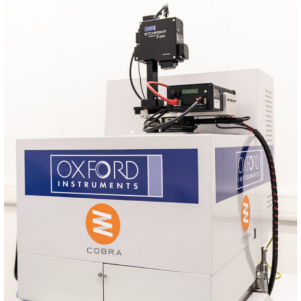
'So, we are happy to see customers gaining benefits from LayTec EtchpointTM. Oxford Instruments’ customer Rohm use it in their HVM process of p-GaN HEMTs, as well as other GaN PE and RF companies'
WOOWON Technology, the exclusive representative of Oxford Instruments Plasma Technology in Korea, works to provide advanced plasma etching and deposition solutions designed for the Korean semiconductor and nanofabrication market. Grant Baldwin, Head of Marketing joins Dr Hwan-won Oh, CEO of Woowon Technology to speak about this important partnership and how Oxford’s state-of-the-art technologies combines with WOOWON’s deep market expertise to deliver innovative solutions.
'...a shared vision to bring cutting edge plasma etching and deposition technologies to our local customers.'
SiC, so long synonymous with high power electronics, is now breaking through the commercial sector as a next-generation material for augmented reality (AR) waveguides. Dr Emma Coleman, technical marketer at Oxford Instruments Plasma Technology, writes about the exciting research emerging from SiC waveguides, the challenges that come with its fabrication and the solutions that Oxford Instruments can provide.
'The adoption of SiC waveguides marks a significant optical breakthrough'

© Oxford Instruments 2026

