 Part of the Oxford Instruments Group
Expand
Collapse
Part of the Oxford Instruments Group
Semi Interface Magazine is Oxford Instruments Plasma Technology’s dedicated publication focusing on the dynamic world of compound semiconductors. Launched to share insight, expertise, and thought leadership, the magazine features contributions from industry professionals, researchers, and our own specialists. Each edition explores insights, trends, innovations, and challenges shaping the sector—spanning topics at the forefront of semiconductor technologies. With a mission to inform and inspire, Semi Interface Magazine is a valuable resource for engineers, scientists, and decision-makers driving the future of the semiconductor industry.
Semi Interface is published three times per year on three topics: wide bandgap power edition in October, opto & datacom in February, and quantum in June. We look forward to bringing you the latest plasma interface engineering and optimisation advances, and thought leadership, in these fascinating high-growth markets.
In this exciting edition, we delve into the groundbreaking innovations and collaborations driving the future of connectivity, AI, AR wearables, silicon photonics, and intelligent machines. From advancements in indium phosphide (InP) technology with Coherent and AOI, to pioneering tailored waveform biasing (TWB) in collaboration with Quantemol, we spotlight the cutting-edge developments shaping semiconductor manufacturing. Plus, explore our new state-of-the-art technical training suite in Bristol, UK, designed to empower our customers with the tools and expertise to optimise performance. Join us as we celebrate the people, technologies, and partnerships transforming our industry.
Explore more
Semi Interface Issue #4: WBG Power Edition explores how silicon carbide (SiC) and gallium nitride (GaN) are transforming power and RF electronics. This issue features global insights into plasma technology advancements, from collaborative innovations in device interface optimisation to industry-leading ALD advancements driving reliability and manufacturability. We also bring you perspectives from global technology experts and highlight SiC’s emerging role in augmented reality, enabling immersive user experiences. Packed with cutting-edge developments, this edition showcases how SiC and GaN are shaping the future as strategic technology platforms across industries.
Explore more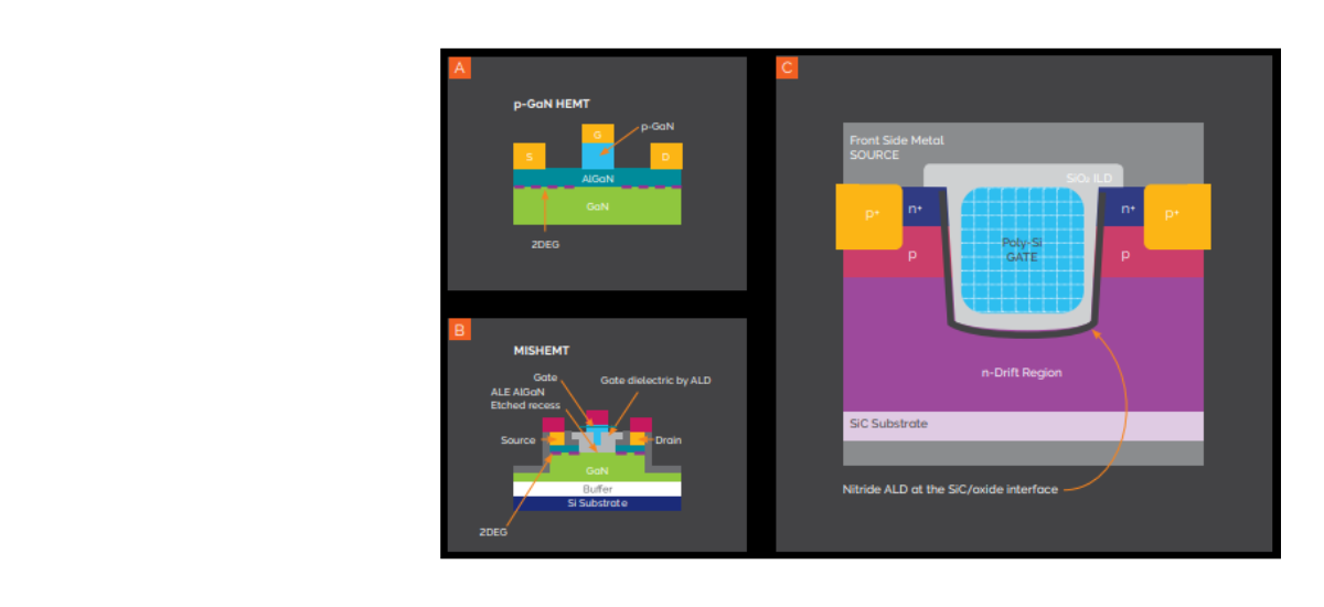
Semi Interface issue 3 focuses on quantum technology during the International Year of Quantum Science and Technology. This edition explores advancements in atomic-scale processing, featuring insights from global leaders like Sir Peter Knight on UK quantum initiatives, updates from Scotland’s University of Glasgow, India’s quantum sensing progress, and interviews with experts from the USA and Australia. We also celebrate 20 years of collaboration with Eindhoven University of Technology, highlight a new MoU, and showcase our cutting-edge ISO5/6 cleanroom with advanced semiconductor metrology capabilities.
Explore more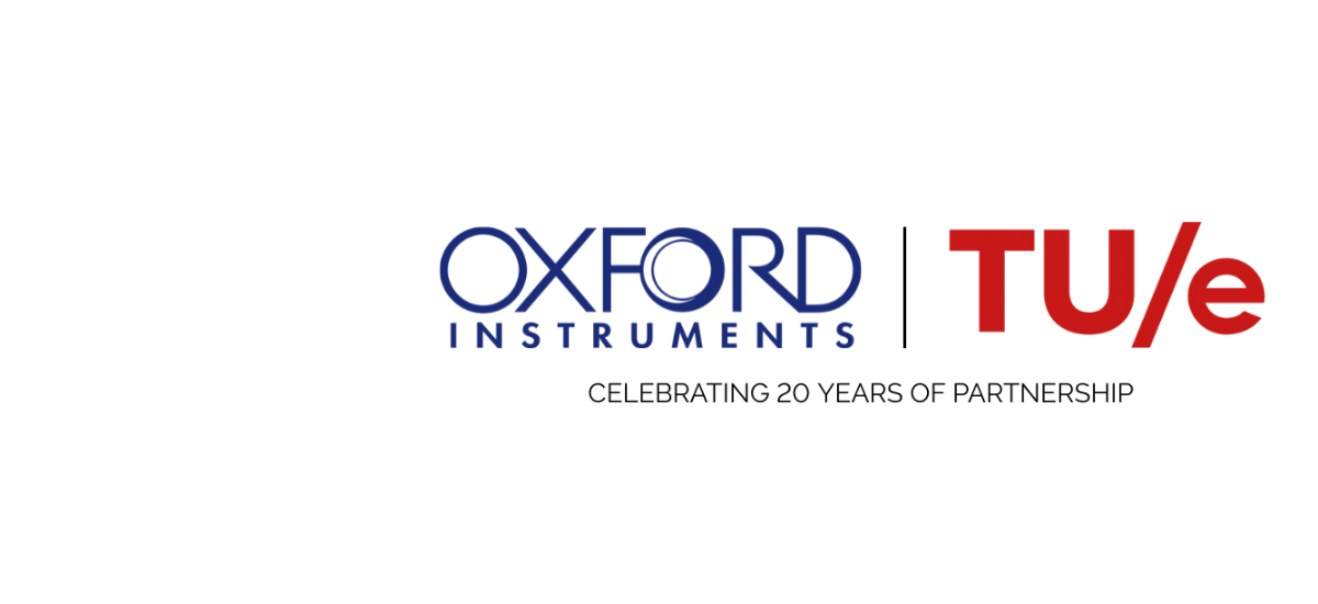
In this issue, our authors explore the significant transformations reshaping the datacom market and examine the technological innovations required to meet the rapidly growing demand for data transceiving devices. The magazine also features expert insights into datacom, microLEDs, augmented reality, and more, offering a comprehensive look at the latest market and technology trends.
Explore more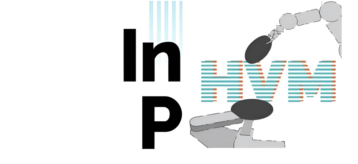
Our contributors bring their extensive expertise to this issue, including a compelling look at how the history of interface optimisation is repeating itself. You'll find in-depth discussions on the latest techniques in interface design and materials engineering, along with forward-looking insights into the interface challenges that lie ahead.
Explore more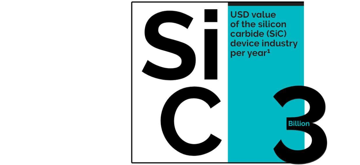
The evolution of power switching and conversion devices is driving breakthroughs in technologies such as electric vehicles and wired/wireless power networks. Materials like Silicon Carbide (SiC) and Gallium Nitride (GaN) are at the heart of these advances, enabling devices that deliver higher efficiency with reduced energy loss.
These Wide Band Gap (WBG) semiconductor devices are at the heart of modern power technologies, enabling fast, high-power switching essential for data transmission in base stations, AI datacentres and green energy applications. GaN and SiC help meet the growing demand for efficient, high-performance power management.
Semi Interface magazine delves into the latest innovations in power device fabrication, highlighting precision processes like plasma etch & deposition, and atomic layer etch (ALE) & atomic layer deposition (ALD). Through expert interviews, in-depth features, and technical insights, each issue showcases how optimised plasma solutions are helping to enhance device performance and lower manufacturing costs across the industry.

This issue explores transformative trends in the opto and datacom markets. In datacom, the explosive growth of generative AI is driving the demand for more devices with higher performance to handle vast data volumes in AI datacentres, prompting a shift to larger wafers and more advanced processes for InP/GaAs datacom transceiver production, supported by scalable, automated manufacturing plasma solutions.
In AR, the fusion of digital and physical worlds is revolutionising fields ranging from surgical navigation to immersive gaming, creating growing demand for ultra-precise, scalable production techniques. The issue highlights how researchers and device production experts leverage cutting-edge technologies like atomic layer etch and deposition (ALE and ALD), advanced ICP etch, and ion beam etch and deposition to achieve high-yielding, high-performing opto and datacom devices.
Quantum technology is ushering in a new era of computing, communication, and sensing by harnessing the unique properties of atoms, electrons, and photons. Manipulating matter into superposition and entanglement enables revolutionary advances, from quantum computing and secure communications, to ultra-precise sensors.
This issue of Semi Interface explores these cutting-edge developments, offering expert interviews, technical features, and insightful editorials on the fabrication of quantum devices. The magazine covers state-of-the-art processes including deep silicon etch for 3D integration, atomic layer deposition of superconducting materials, and precision plasma etch and atomic layer etch for diamond and photonic components. Through diverse content, readers gain an understanding of how advanced wafer-level plasma processing solutions are shaping the future of quantum technologies.


© Oxford Instruments 2026

