 Part of the Oxford Instruments Group
Expand
Collapse
Part of the Oxford Instruments Group
We’re excited to bring you Semi Interface Issue #5: Opto datacom Edition, where we explore the innovations and collaborations shaping the future of technology. In this edition, we highlight the exciting breakthroughs that are advancing AI, AR wearables, silicon photonics, and more—pushing the boundaries of connectivity, datacentres, and intelligent machines.
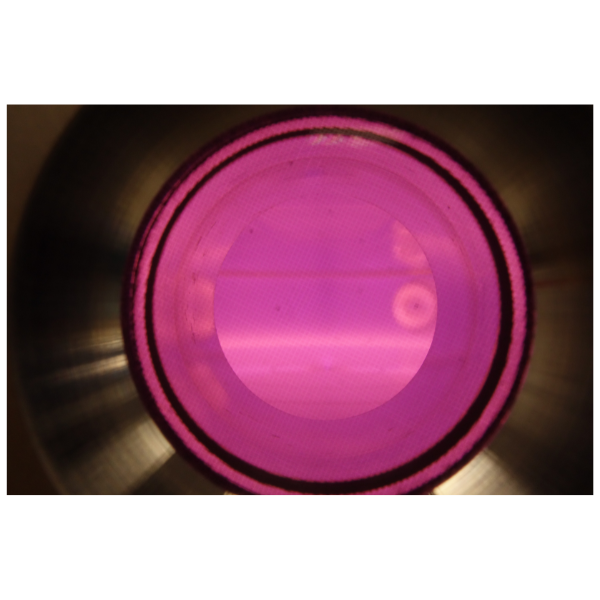
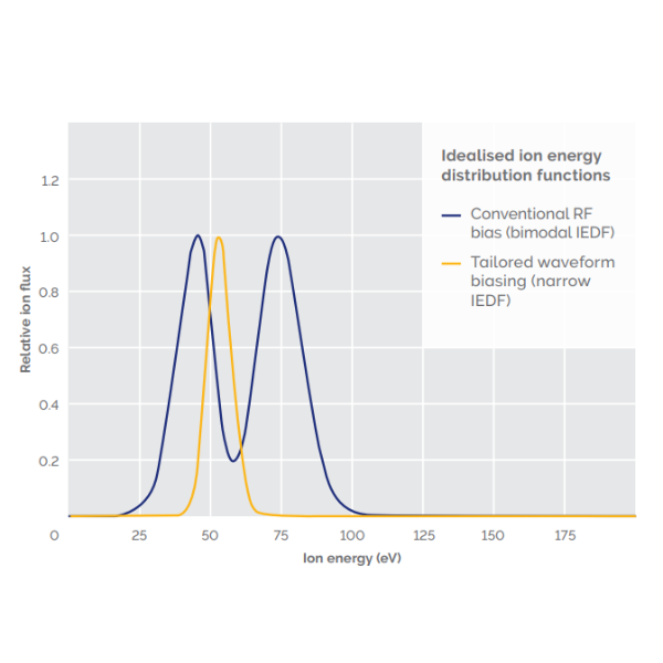
At Oxford Instruments, we are privileged to work alongside industry leaders and researchers to tackle some of the most complex challenges in semiconductor manufacturing. Working with Coherent and AOI, we are at the leading-edge of indium phosphide (InP) technology, including 6-inch wafer processing. Our collaboration with Quantemol on tailored waveform biasing (TWB) could enable next-generation fabrication capability, which is an exciting development in plasma innovation.
We also shine a spotlight on our new state-of-the-art technical training suite in Bristol, UK, designed to empower our customers with the skills and knowledge to optimise system performance and operational efficiency. Join us as we share these stories and more, highlighting our service strategy, people, technologies, and partnerships driving industry transformation.
Download magazine
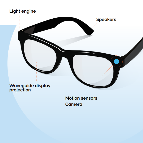
Mixed reality (MR) and AI glasses are evolving rapidly, seamlessly blending physical and digital realities. However, challenges such as high costs, bulkiness, limited consumer appeal, and privacy concerns persist. Discover how Oxford Instruments is tackling these issues with ground breaking innovations in diffractive waveguide technology.
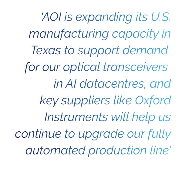
Oxford Instruments has partnered with Applied Optoelectronics Inc. (AOI) to enhance U.S. production of advanced indium phosphide (InP) optoelectronic devices. As AOI expands its Texas operations to meet growing demand for optical transceivers in AI datacenters, Oxford Instruments will provide cutting-edge plasma processing systems to improve efficiency, quality, and scalability. This collaboration underscores both companies' dedication to driving innovation in next-generation optoelectronic manufacturing.
Oxford Instruments is supporting Coherent Corp. in achieving the first fully automated 6-inch indium phosphide (InP) wafer fabrication capability. The shift to 6-inch wafers enhances production capacity, reduces die costs, and supports AI datacentres, telecommunications, and sensing technologies. This collaboration is paving the way for next-generation InP optoelectronic devices.
Oxford Instruments and Quantemol have partnered on an Innovate UK-backed project to advance plasma etching technology. By optimising ion energy control through tailored waveform biasing (TWB), the collaboration aims to reduce energy consumption, minimise waste, and enhance precision in semiconductor fabrication.
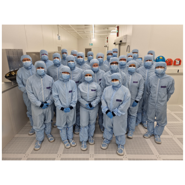
Step into the future of technical training! Oxford Instruments has unveiled a state-of-the-art technical training suite in Bristol, UK, offering hands-on programmes in plasma etch, deposition, atomic layer etch (ALE), atomic layer deposition (ALD), and ion beam etch and deposition. With flexible delivery options, these courses empower customers to optimise system performance, minimise downtime, and enhance operational safety.
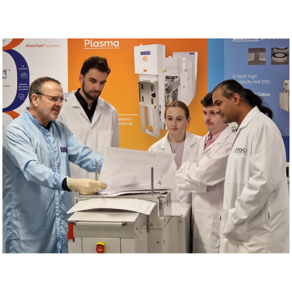
Service excellence is the cornerstone of innovation. Oxford Instruments is redefining service with a proactive approach, emphasising preventive maintenance, technical training, and lifecycle support. Backed by a global team, the company is committed to delivering consistent, high-quality support to customers worldwide.
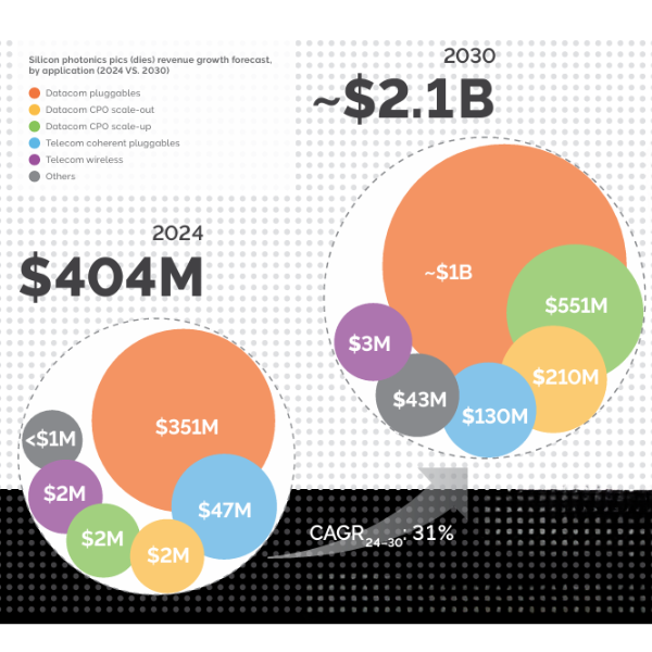
Silicon photonics is emerging as a transformative technology for next-generation connectivity, driven by AI, hyperscale datacentres, quantum computing, and medical imaging. The market for silicon photonics-based modules is projected to grow from $4.2 billion in 2024 to $24.8 billion by 2030 (35% CAGR). Explore how materials innovation, including SOI, SiN, LNOI, and InP platforms, is driving advancements in bandwidth, modulation, and coherent communication channels.
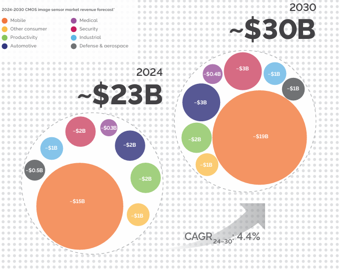
The CMOS image sensor (CIS) industry is evolving, with global revenues rebounding by 6.4% year-on-year in 2024. Automotive, security, and surveillance sectors are becoming key growth drivers, while emerging architectures like digital pixel sensors (DPS) enable better sensitivity and adaptive sensing. Learn how CIS technology is powering the shift to intelligent, AI-enhanced smart machines.
SMART Photonics is leading Europe’s photonics revolution with advanced indium phosphide (InP) photonic integrated circuits (PICs). Recent upgrades, including the move from 3-inch to 4-inch wafers, have doubled production capacity and reduced costs. Learn how collaborations with academia, industry, and government are accelerating developments in AI datacentres, 5G/6G networks, LiDAR, and medical diagnostics.

Join Prof. Peter Smowton as he discusses the pivotal role of compound semiconductors in revolutionising optoelectronics. From quantum dots and silicon integration to advancements in datacentres, healthcare, and robotics, discover how cutting-edge research is bridging the gap between academia and industry to foster innovation and scalability.
Tailored waveform biasing (TWB) is revolutionising semiconductor manufacturing by enabling precise ion energy control. Oxford Instruments and Quantemol are collaborating on an Innovate UK-supported project to explore TWB’s applications in next-generation fabrication processes like atomic layer etching (ALE), with a focus on improving energy efficiency and minimising material waste.

© Oxford Instruments 2026

