Part of the Oxford Instruments Group
Expand
Collapse
Part of the Oxford Instruments Group
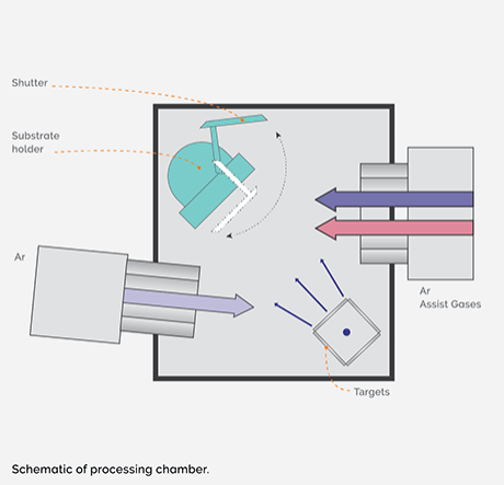
Ion Beam Deposition (IBD) provides an exceptionally versatile approach to deposition. Our ion beam deposition products are chosen for their ability to produce deposited films with high quality, dense and smooth surfaces.
Our systems have flexible hardware options including open load and cassette to cassette. System specifications are closely tuned to applications, enabling faster and repeatable process results.
Properties, such as refractive index, absorption, scattering, adhesion and packing density, can be tuned by varying beam parameters such as beam flux and energy, platen orientation relative to incoming materials and gas flow.
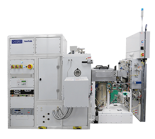
Our ion beam deposition (IBD) system is a popular choice for high-quality material processing. Our systems have flexible hardware options including single substrate load lock and cassette to cassette. System specifications are closely tuned to applications, enabling faster and repeatable process results.
View full hardware specification >
As well as our IBD technology, we also offer ion beam etching (IBE) solutions.
Ion Beam Etching (or milling) is achieved by directing a beam of charged particles (ions) at a substrate with a suitably patterned mask in a high vacuum chamber. It enables highly-directional beams of neutral ions to control over the sidewall profile as well as radial uniformity optimisation and feature shaping during nanopatterning.
Our Ionfab Ion Beam system is capable of both IBE and IBD technology.
FIND OUT MORE
© Oxford Instruments 2026