Part of the Oxford Instruments Group
Expand

Powerful Plasma Deposition Solutions

Discover our industry-leading plasma deposition PECVD & ICPCVD solutions and systems.

PECVD Solutions

Plasma-enhanced CVD, or PECVD, is a well-established technique for deposition of a wide variety of films. Many types of device require PECVD to create high-quality passivation or high density masks.

The PECVD process modules are specifically designed to produce excellent uniformity and high rate films, with control of film properties such as refractive index, stress, electrical characteristics and wet chemical etch rate.

ICPCVD Solutions

Inductively Coupled Plasma Chemical Vapour Deposition, ICPCVD. Creation of high-density plasmas in the ICP source means this technique delivers deposition of high-quality dielectric films at low temperature with low damage.

Low temperature deposition means that temperature-sensitive films and devices can be processed successfully.

Key Benefits of PECVD

  • Top electrode RF driven (MHz and/or kHz); no RF bias on lower (substrate) electrode 
  • Substrate sits directly on heated electrode 
  • Gas injected into process chamber via “showerhead” gas inlet in the top electrode 
  • Film stress can be controlled by high/low frequency mixing techniques 
  • Lower temperature processes compared to conventional CVD
PECVD diagram

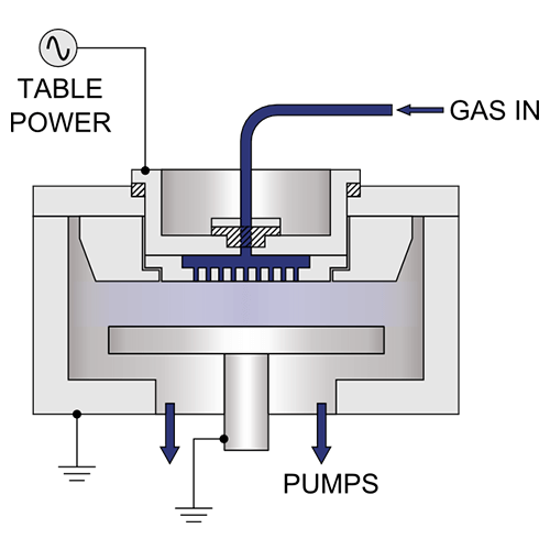
PECVD process and chamber diagram

Key Benefits of ICPCVD

  • Independent control of ion energy and ion current density
  • Typical process pressure: 1- 10 mtorr
  • Plasma density: >1011 cm-3
  • Plasma in contact with the substrate
  • Low energy ion current during deposition
  • Ion Current (Plasma Density) dependent on ICP power
  • ESS (electrostatic screen) for a purely inductive plasma
  • ICP is fully automatic (2 RF automatch units)
ICPCVD diagram

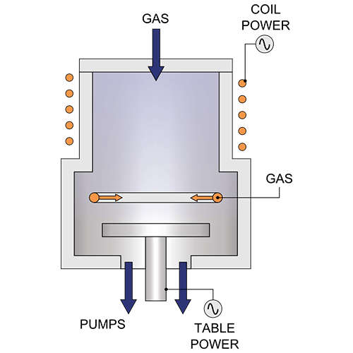
ICPCVD process and chamber diagram

Applications

  • High quality PECVD of silicon nitride and silicon dioxide for photonics, dielectric layers, passivation and many other uses
  • Hard mask deposition and etch for high brightness LED production
  • VCSEL manufacturing
  • Diamond-like Carbon (DLC) deposition

Processes

  • Typical materials deposited include SiO2Si3N4 and SiON, Si and SiC at substrate temperatures as low as 5ºC

We have developed a process library of over 7,000 recipes. Speak to one of our experts today to discuss your process requirements.

REQUEST MORE INFO

PlasmaPro Systems for PECVD

PlasmaPro 80 PECVD

PlasmaPro 80 PECVD

  • Open load design allows fast wafer loading and unloading
  • Excellent wafer temperature uniformity
  • Up to 200mm wafers
  • Low cost of ownership
  • Built to Semi S2/S8 standards

Full product specification >

PlasmaPro 100 PECVD

PlasmaPro 100 PECVD

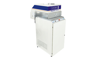
  • High-quality films, high throughput, excellent uniformity

  • Compatible with all wafer sizes up to 200mm
  • Rapid change between wafer sizes
  • Low cost of ownership and ease of serviceability
  • Resistive heated electrodes with capability up to 400°C or 1200°C

Full product specification >

PlasmaPro 800 PECVD

PlasmaPro 800 PECVD

  • High-performance processes
  • Excellent substrate temperature control
  • Precise process control
  • Proven processes for 300mm single wafer Failure Analysis

Full product specification >


PlasmaPro Systems for ICPCVD

PlasmaPro 80 ICPCVD

PlasmaPro 80 ICPCVD

  • Open load design allows fast wafer loading and unloading
  • Excellent etch control and rate determination
  • Excellent wafer temperature uniformity
  • Up to 200mm wafers
  • Low cost of ownership
  • Built to Semi S2/S8 standards

Full product specification >

PlasmaPro 100 ICPCVD

PlasmaPro 100 ICPCVD

  • Excellent uniformity, high throughput and high precision processes

  • High quality films
  • Wide temperature range electrode
  • Compatible with all wafer sizes up to 200mm
  • Rapid change between wafer sizes
  • Low cost of ownership and ease of serviceability

Full product specification >

PECVD & ICPCVD Systems Comparison

PlasmaPro 80 PlasmaPro 100 PlasmaPro 800
Technology PECVD & ICPCVD PECVD & ICPCVD PECVD
Electrode size 240mm 460mm
Substrates Up to 240mm diameter Up to 200mm diameter Up to 460mm diameter
Dopants No Various available No
Liquid precursors No Yes (TEOS) No
MFC controlled gas lines 4, 8 or 12 line gas box available
Wafer stage temperature range 20°C to 400°C 20°C to 1200°C 20°C to 400°C
In-situ plasma clean Yes Yes Yes
REQUEST A QUOTE

Related Content

Questions? Ask our experts today for more information.

CONTACT US