 Part of the Oxford Instruments Group
Expand
Collapse
Part of the Oxford Instruments Group
Efficient power switching and conversion devices are used to make possible new technologies such as electric cars and local power creation and distribution networks.
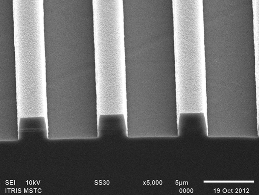
Advances in device performance through use of materials such as SiC and GaN means lower energy losses. Oxford Instruments has a deep understanding of how to make the most optimised devices through its process solutions such as atomic layer deposition, plasma etching and plasma deposition.
DOWNLOAD BROCHURESimplified process flow. Orange processes show solutions covered by Oxford Instruments' technology.
Atomfab is our latest innovation in ALD system technology, delivering fast pace, low damage, low CoO production plasma ALD processing for GaN power and RF devices.
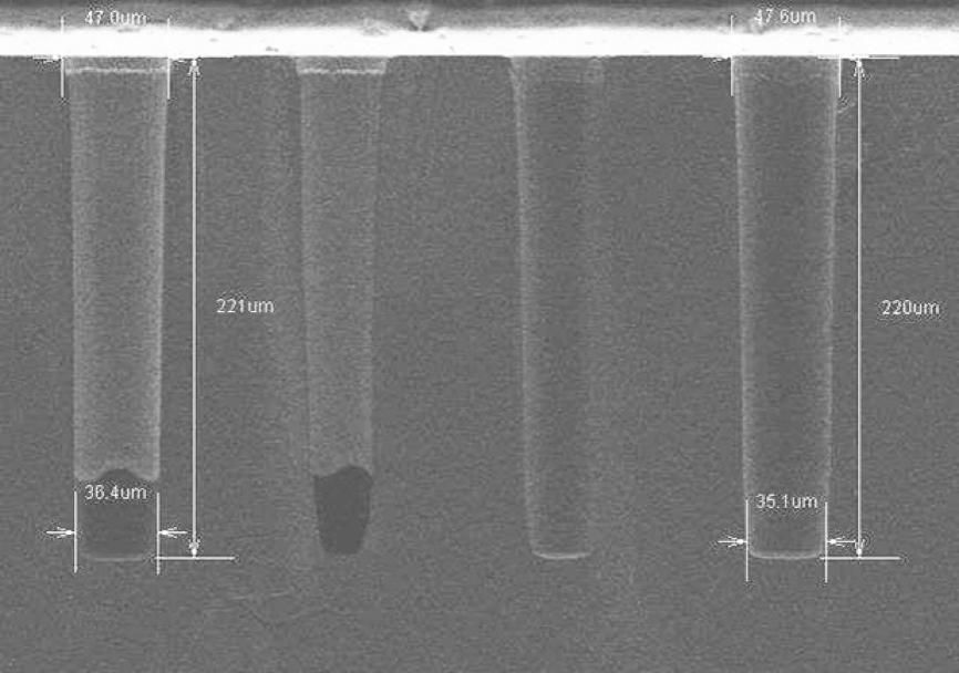
SiC hole etch SEM image
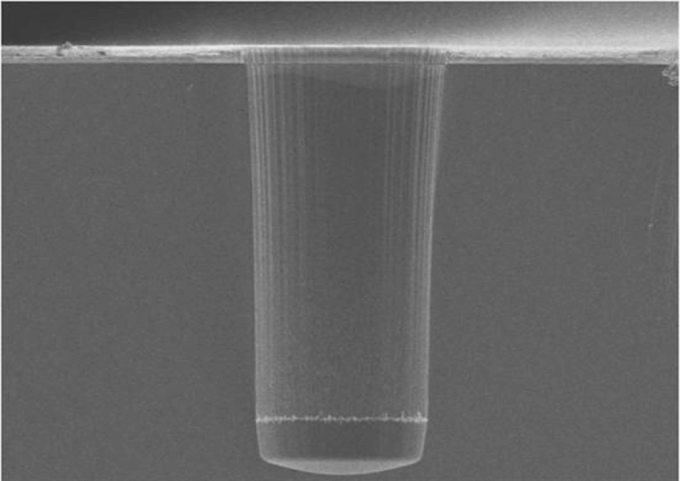
SiC hole etch close-up SEM image
Smooth and vertical SiC feature etch

© Oxford Instruments 2026

