

Oxford Instruments enables ROHM’s in-house GaN manufacturing with…
Oxford Instruments, a leading provider of advanced plasma processing solutions…
 Part of the Oxford Instruments Group
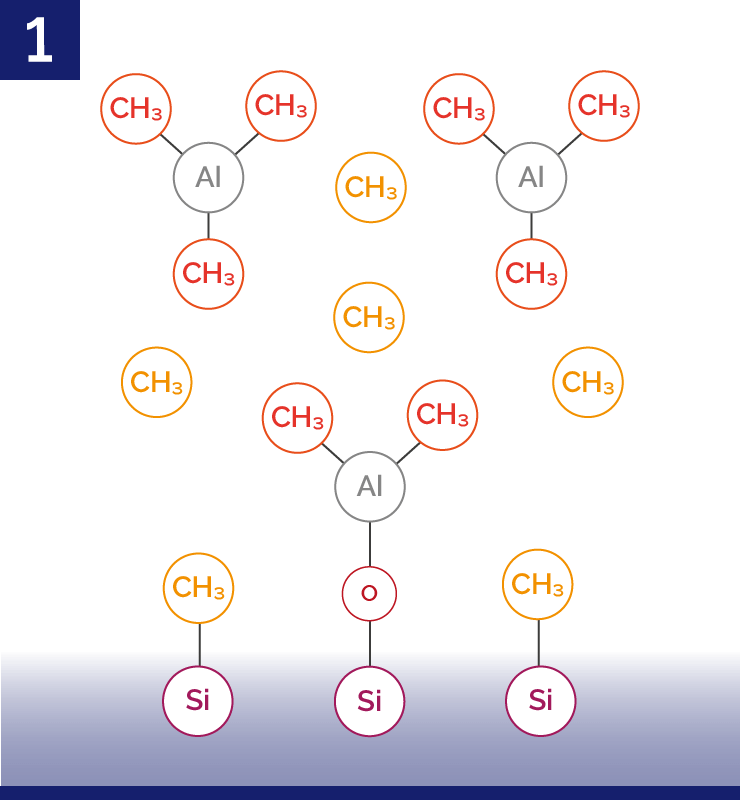
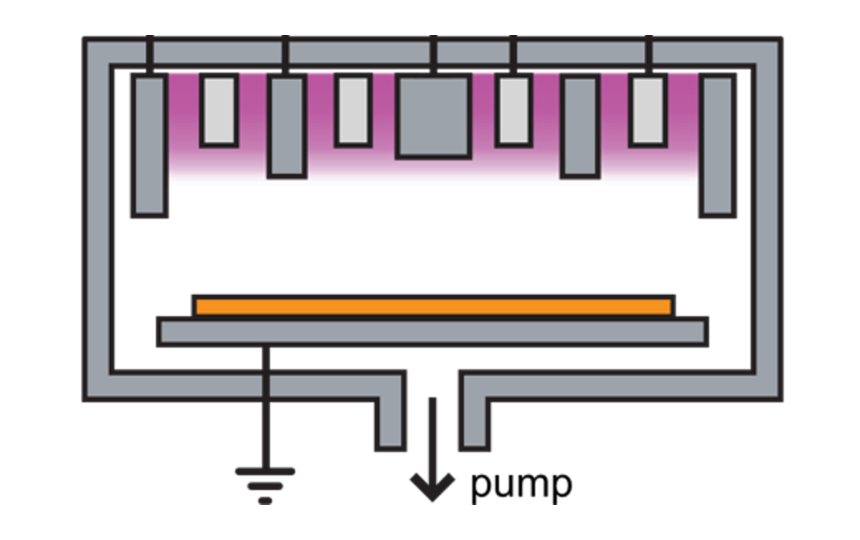
ALD typically involves a cycle of 4 steps that is repeated as many times as necessary to achieve the required deposited thickness. The example below shows ALD of Al2O3 using Al(CH3), (TMA) and O2 plasma.
Step 1) Dosing of the substrate with a precursor vapour of TMA, which adsorbs on and reacts with the surface. With the correct choice of precursor and parameters, this reaction is self-limiting.
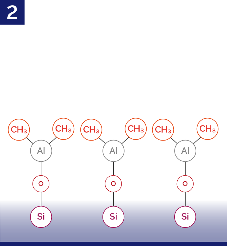
Step 2) Purging of all residual precursor and reaction products.
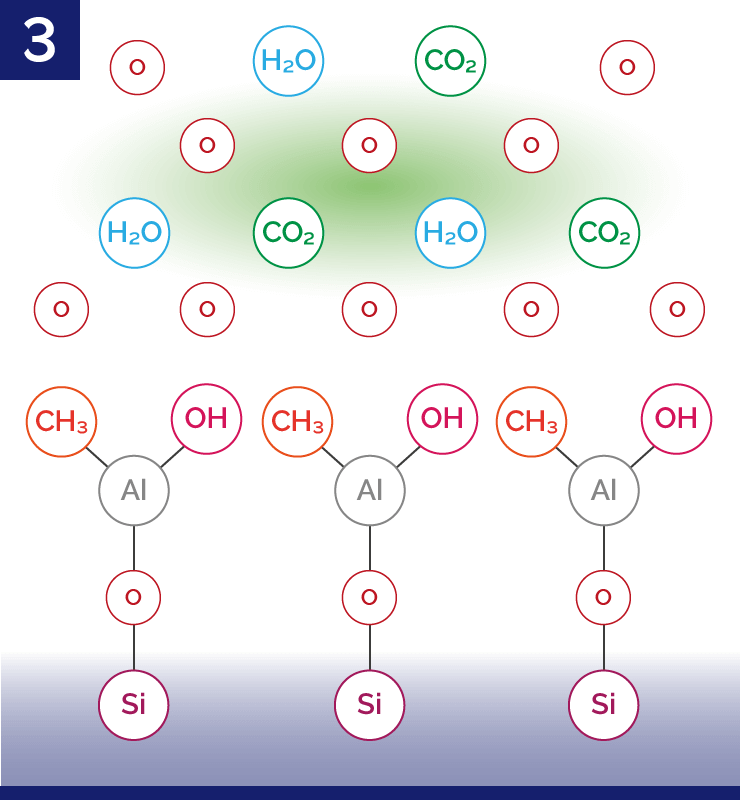
Step 3) Low damage remote plasma exposure to the surface with reactive oxygen radicals which oxidise the surface and remove surface ligands. This reaction is self-limiting due to the limited number of surface ligands.
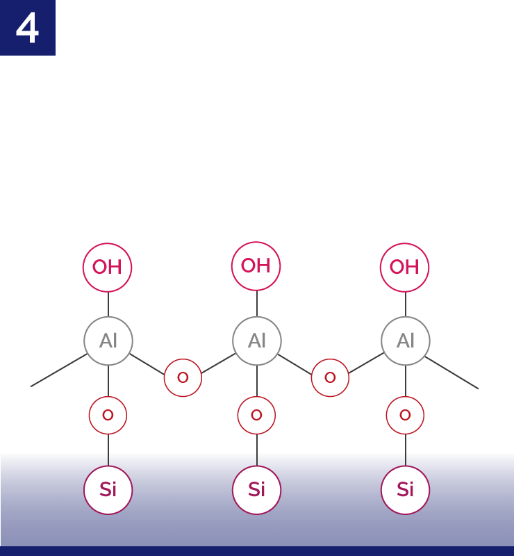
Step 4) Reaction products are purged from the chamber.
Only step 3 varies between H2O for the thermal process or O2 plasma. As the ALD process deposits a (sub)angstrom thickness per cycle, control over the deposition process is obtained at the atomic scale.
1st half-cycle
Purge
2nd half-cycle
Purge
ALD is an advanced deposition technique that allows for ultra-thin films of a few nanometres to be deposited in a precisely controlled way. Not only does ALD provide excellent thickness control and uniformity, but 3D structures can be covered with a conformal coating for high-aspect-ratio structures.
ALD relies on self-limiting surface reactions and therefore generally provides very low pin-hole and particle levels, which can benefit a wide range of applications. The level of film/interface control and high film quality provided are sought after for many applications. The usage of plasma allows for improved film properties, control thereof and a wide range of possible materials. The flexibility of unique surface pre-treatments allows for low damage processing.

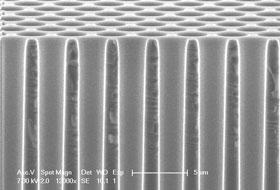
Conformal coating of high aspect ratio (15:1) structure with high-rate plasma ALD SiO2
Al2O3 deposited by FlexAL ALD - Courtesy by Eindhoven University of Technology
In addition to the benefits of thermal ALD, plasma enhanced (PEALD) allows for a wider choice of precursor chemistry with enhanced film quality:
Conformal deposition of SiO2, TiO2 and Al2O3 by plasma ALD, (CC BY 4.0 license), image library at www.AtomicLimits.com, 2021
2D materials growth can also be grown by ALD which is a new development with the aim to go toward high-quality transition metal dichalcogenide (TMD) films. ALD chemistry control has the promise to be able to utilise 2D TMDs (both n-type and p-type) with their unique properties at CMOS compatible temperatures with precise digital thickness control over a large area (200 mm wafers).
A wide variety of materials is possible with ALD and a wide range of processes can be guaranteed and set up by our process engineers. For novel processes, our extensive process knowledge and vast network allow us to provide starting point recipes that should be good starting blocks to go quickly towards a robust process.
Often plasma-based processes are available utilising our plasma knowledge and handling of mass flow controller (MFC) gas mixtures including toxic gases.
Metals |
Fluorides |
Sulfides |
Selenides |
Pt |
AlF3 |
MoS2 |
MoSe2 |
Ru |
MgF2 |
WS2 |
WSe2 |
Oxides |
Nitrides | |
Al2O3 |
| |
Co3O4 |
||
Ga2O3 |
GaN | |
HfO2 |
HfN | |
In2O3 |
||
Li2CO3 |
||
MoO3 |
||
Nb2O5 |
| |
NiO |
||
SiO2 |
Si3N4 | |
SnO2 |
||
Ta2O5 |
TaN | |
TiO2 |
TiN | |
WO3 |
WN | |
ZnO |
||
ZrO2 |
Solutions for your productions needs:
Atomfab's ALD technology offers precisely controlled ultra‑thin films for advanced applications on the nanometre scale, with conformal coating of sensitive substrate structures.
Read more about how ALD can optimise GaN power devices in our white paper.
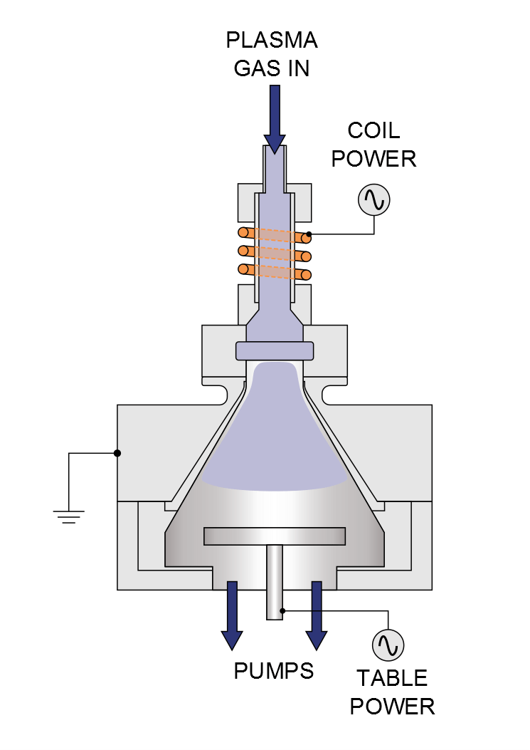
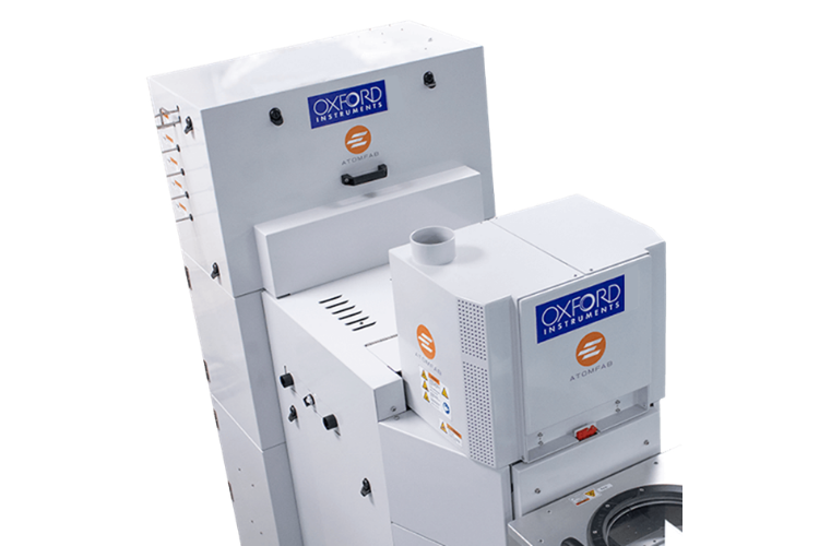
Revolutionary plasma source: Atomfab system uses a patent pending remote source specifically designed for atomic scale processing.
Plasma ALD Al2O3 at 300 °C |
Specification |
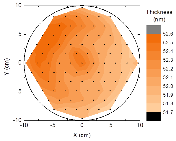
Within wafer thickness uniformity |
<±1.0% |
Wafer-to-wafer thickness repeatability |
<±1.0% |
Breakdown voltage |
≥7.0 MV/cm |
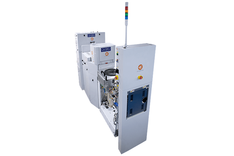
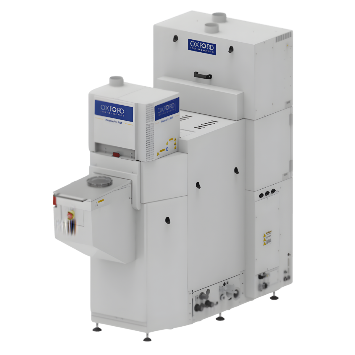
Based on production-proven platform for corporate/specialised R&D, PlasmaPro ASP has been designed to ensure high quality materials that can be deposited at speed with flexibility to run multiple chemistries to give excellent layers for incorporation into devices. Our cutting-edge plasma enhanced ALD (PEALD) system offers flexibility, conformality, and tunability of ALD with speed for higher throughput and thicker films.
Faster than conventional remote plasma
PlasmaPro ASP has shared platform with Atomfab to deliver fast and low damage remote PEALD. Remote PEALD offers superior device performance compared to thermal ALD and direct plasma ALD. It is compact to limit the effective chamber volume for rapid gas exchange and it is effective over the full 200 mm wafer diameter.
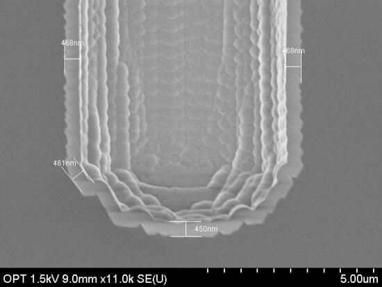
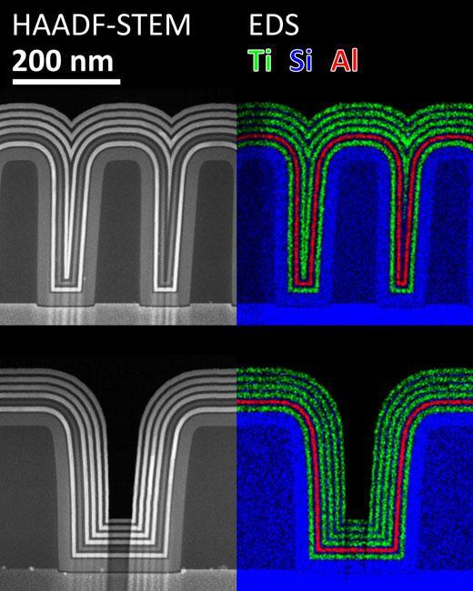
450 nm conformal SiO2 deposited in 32:1 aspect ratio trench using PlasmaPro ASP.
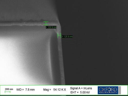
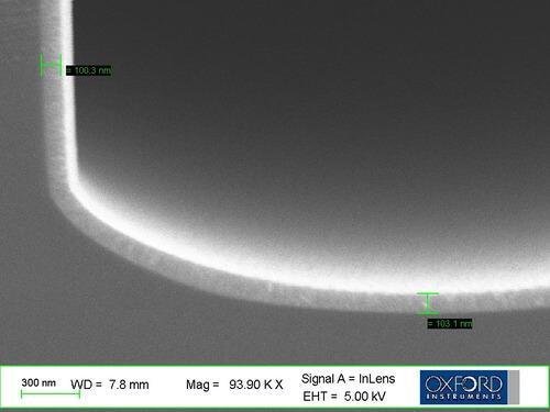
130 nm conformal superconducting NbN deposited in 8:1 aspect ratio trench using PlasmaPro ASP.
Specifications |
PlasmaPro ASP |
Precursor lines |
Maximum 6 (any combination) |
Precursor size (ml) |
200 |
Precursor type |
|
Handling |
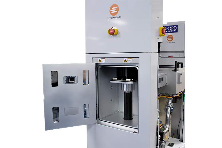
Loadlock |
Gas pod |
4 Process + 1 Ar (onboard) |
Electrode |
400 °C grounded/ biased |
Roughing pump |
600 m3/hr |
Compliance |
UL Standard, designed for SEM 2S |
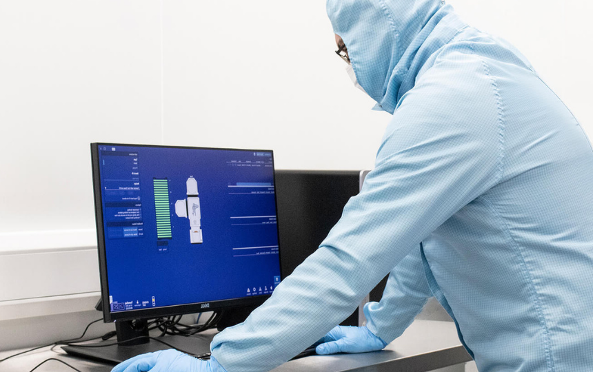
Software |
PTIQ |
PEALD process library |
Al2O3, SiO2, NbN, TiN, more in development |
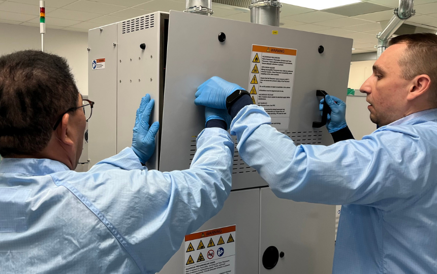
Oxford Instruments is committed to providing a comprehensive, flexible and reliable global customer support. We offer excellent quality service throughout the life of your system.
PTIQ is the latest intelligent software solution for PlasmaPro and Ionfab processing equipment.
At Oxford Instruments Plasma Technology, we offer a wide range of technical training courses designed to suit all skill levels and needs.

© Oxford Instruments 2026