Part of the Oxford Instruments Group
Expand
Collapse
Part of the Oxford Instruments Group
2D materials are at the very limit of thin-film dimensions with thicknesses down to a single atom. While graphene kick-started exploration and application of these ultra-thin materials, it has created a vast field of exploration and application of several other 2D materials like nitrides (hBN) and transition metal dichalcogenides (MoS2, WSe2 etc.).
While these materials can be found in nature and can be exfoliated from the bulk crystals, chemical vapour-based techniques are employed to allow easy scale-up for future devices.
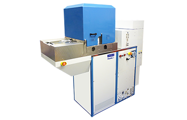
DOWNLOAD BROCHUREOrange processes show solutions covered by Oxford Instruments' technology.
2D materials exhibit superlative electronic and optoelectronic properties which researchers today are working on harnessing for next-generation devices for electronics, optoelectronics and flexible devices.
Various aspects of 2D materials can be beneficial for applications and depending on the application people might aim for single layers with high mobility for transistors or multiple layers in many orientations for catalysis applications, such as water splitting.
2D materials such as graphene, MoS2 or hBN can be used to enhance current devices and build new device architectures. FETs, batteries and filters with unique properties can now be realised.
At Oxford Instruments Plasma Technology we have excellent experience with a wide range of processes, from high-temperature CVD to low-temperature ALD.
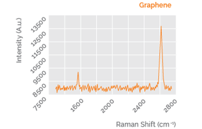
This specification is issued for Graphene obtained through Chemical Vapour Deposition (CVD) processes.
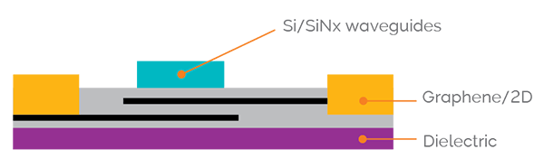
Graphene EO modulator for datacom.
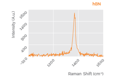
This specification is issued for Boron Nitride obtained through Chemical Vapour Deposition (CVD) processes. For the purpose of process demonstration, B2H6 is used as Boron source and NH3 as the Nitrogen sources on Cu/Ni foils as catalyst substrates.
We offer PECVD systems equipped with precursor vapour delivery modules for the growth of two-dimensional layers of materials like MoS2, WS2 etc.
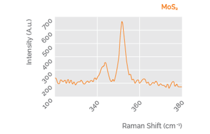
Excellent thickness control with low defects and strong photoluminescence
High-quality MoS2:

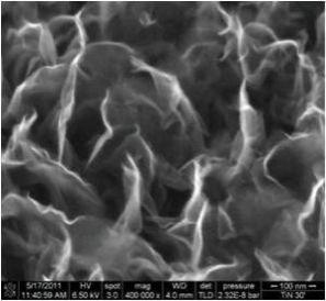
Direct growth of nanocrystalline Graphene on dielectric substrates using plasma-enhanced chemical vapour deposition.
In situ growth of 2D Molybdenum Disulphide (MoS2) Graphene heterostructures
We offer CVD/PECVD/Remote plasma (ICP) CVD systems equipped with precursor vapour delivery modules for the growth of two-dimensional layers and heterostructures of materials like Graphene, MoS2, WS2 etc.
This is a three-step process:
For more information, speak to our experts today.
REQUEST MORE INFOFor atomic layer deposition approaches to 2D materials, our FlexAL system can be specifically configured to allow growth of 2D transition metal dichalcogenides, such as MoS2. The FlexAL is ideal for growing metal oxide seed layers for sulfurization, deposition of high-k dielectrics, surface pretreatments and 2D materials encapsulation.
Find out more about FlexAL.
FlexAL ALD system for 2D materials beyond graphene.

© Oxford Instruments 2025