

Oxford Instruments enables ROHM’s in-house GaN manufacturing with…
Oxford Instruments, a leading provider of advanced plasma processing solutions…
 Part of the Oxford Instruments Group
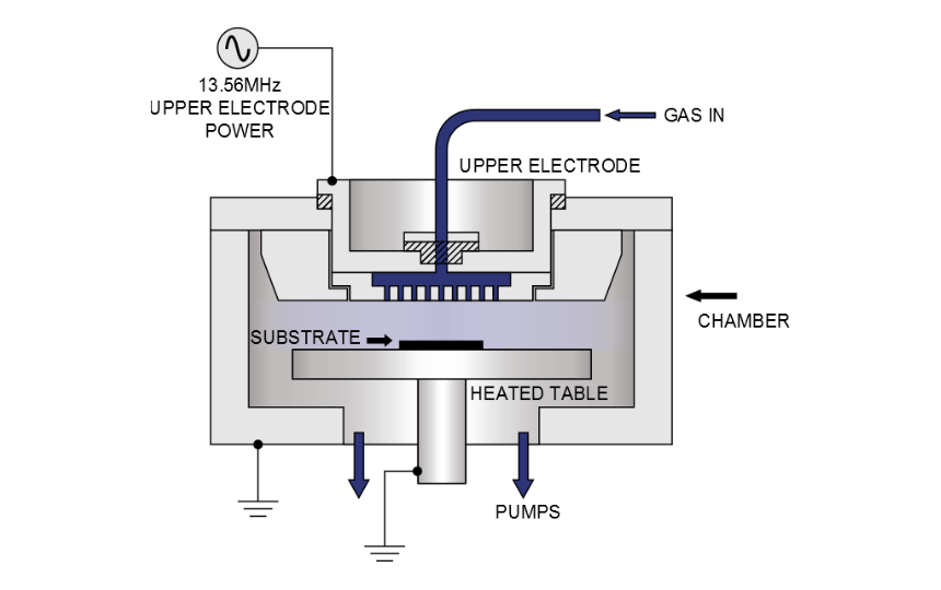
CVD is a well-established technique for deposition of a wide variety of films with different compositions and thicknesses down to a single layer of atoms.
This specification is issued for graphene obtained through CVD processes.
This specification is issued for hBN obtained through CVD processes. For the purpose of process demonstration, B2H6 is used as boron source and NH3 as the nitrogen sources on Cu/Ni foils as catalyst substrates.
We offer PECVD systems equipped with precursor vapour delivery modules for the growth of 2D layers of TMD materials like MoS2, WS2 etc.
Excellent thickness control with low defects and strong photoluminescence
High-quality MoS2:
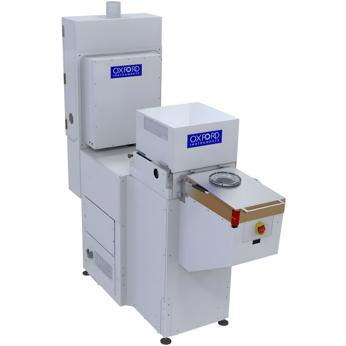
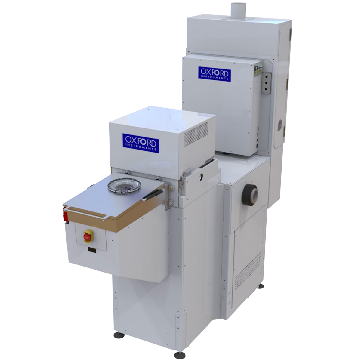
CVD & ALD tools for growth of 1D/2D nanomaterials and heterostructures. PlasmaPro 100 Nano (formerly Nanofab) delivers high-performance growth of nanomaterials with in-situ catalyst activation and rigorous process control, with flexible temperatures up to 1,200 °C.
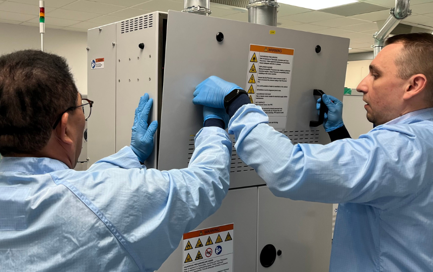
Oxford Instruments is committed to providing a comprehensive, flexible and reliable global customer support. We offer excellent quality service throughout the life of your system.
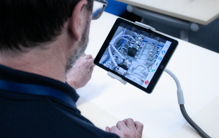
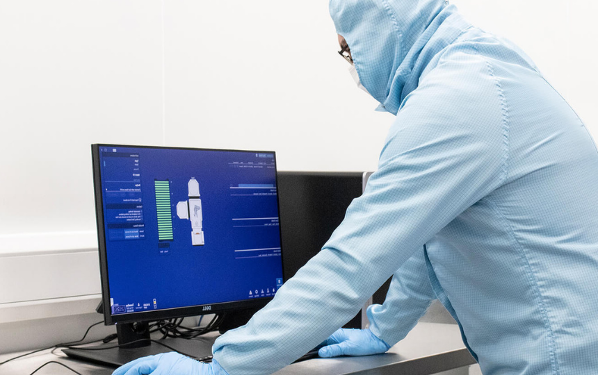
PTIQ is the latest intelligent software solution for PlasmaPro and Ionfab processing equipment.
At Oxford Instruments Plasma Technology, we offer a wide range of technical training courses designed to suit all skill levels and needs.

© Oxford Instruments 2026