Part of the Oxford Instruments Group
Expand

Powerful ALD & ALE Atomic Scale Processing Solutions

Discover our industry-leading plasma-enhanced atomic scale processing solutions with ALD and ALE technology.

Atomic Layer Deposition (ALD) Solutions

Atomic Layer Deposition (ALD) is an advanced deposition technique that allows for ultra-thin films of a few nanometres to be deposited in a precisely controlled way. Not only does ALD provide excellent thickness control and uniformity but 3D structures can be covered with a conformal coating for high-aspect-ratio structures.

Key Benefits of ALD

  • Self-limiting atomic layer-by-layer growth
  • Highly-conformal coating
  • Low pin-hole and particle levels
  • High-quality oxides with low damage
  •  Low-temperature process for sensitive substrates
  • Metals with low nucleation delay
  • Wide range of materials and processes

In addition to the benefits of thermal ALD, plasma ALD allows for a wider choice of precursor chemistry with enhanced film quality. It offers:

  • Low-temperature processes and the remote source maintains low plasma damage
  • Eliminates the need for water as a precursor, reducing purge times between ALD cycles
  • Higher quality films through improved removal of impurities for lower resistivity and higher density


Applications

  • Quantum Technology
    • Superconducting materials for qubits, quantum circuits and single-photon detectors
    • Oxides such as Al2O3 and HfO2 for tunnel barriers in Josephson Junctions
  • 2D Materials
    • Deposition of TMDs such as Mos2 and Ws2
  • GaN Power
    • Passivation of GaN/AlGaN power devices
  • Biomedical Devices
    • Microfluidics
    • Active devices
    • Hermetic/Biocompatible coatings

Find out more about the atomic layer deposition process >

DOWNLOAD BROCHURE REQUEST MORE INFO
ALD SiO2 SEM

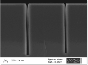
Conformal coating of high aspect ratio (15:1) structure with high-rate plasma ALD SiO2.

ALD AL2O3 SEM

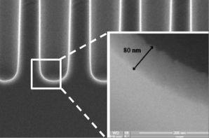
80 nm remote plasma ALD Al2O3 film in 2.5 mm wide trenches with aspect ratio ~10, deposited with FlexAL.

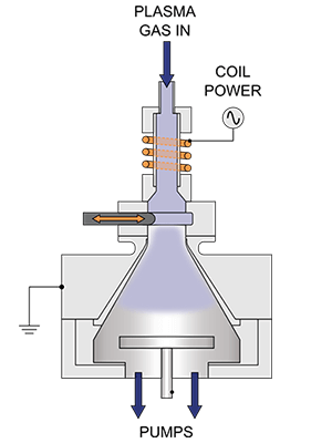
ALD processing chamber.

Atomic Layer Deposition Systems

FlexAL

FlexAL

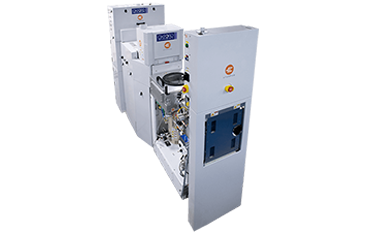
The FlexAL atomic layer deposition (ALD) system offers a broad range of optimised high-quality plasma ALD and thermal ALD processes with maximum flexibility in precursors, processes gases, and hardware configuration within a single process chamber.

  • RF biased electrode option available for control of film properties

  • Industry-standard cassette to cassette handling for higher throughput

  • Maximum flexibility in the choice of precursors, process gases, hardware features and options

  • Optimised to maintain low-damage, high-quality substrates

  • Low temperature to enable high-quality deposition on temperature-sensitive surfaces
MORE INFORMATION

Atomfab

Atomfab

Specifically designed for high-volume manufacturing, Atomfab delivers fast, low damage, low CoO production plasma ALD processing for GaN power and RF devices.

Atomfab offers precisely controlled ultra‑thin films for advanced applications on the nanometre scale, with conformal coating of sensitive substrates structures.

  • Competitive CoO
  • Quick, easy maintenance
  • Up to 200 mm wafer handling with cluster configuration options
  • Excellent film uniformity
  • High material quality
  • Low substrate damage
MORE INFORMATION

Atomic Layer Etching (ALE) Solutions

Atomic Layer Etching (ALE) is an advanced etch technique that allows for excellent depth control on shallow features. As device feature size reduces further and further ALE is required to achieve the accuracy required for peak performance.

Plasma-based atomic layer etching is a cyclical etching process of gas dosing and ion bombardment that removes material layer by layer and has the potential to remove single atomic layers with very low damage.

Key Benefits of ALE

  • Smooth etch surfaces
  • High selectivity
  • Low damage etching with low ion energies
  • Precise control and high accuracy of etching depth
  • Excellent uniformity
  • Minimal aspect ratio dependence

Applications

  • MEMS & Sensors
  • Optoelectronics
  • Discrete power devices
  • 2D materials

Processes

  • III-V etch processes
  • Solid-state lasers with InP etching
  • VCSEL GaAs/AlGaAs etch
  • RF device low damage GaN etch
  • Silicon bosch and cryo-etch processes
  • SiO2 and quartz etch

Find out more about the atomic layer etching process >

DOWNLOAD BROCHURE REQUEST MORE INFO
Si 25nm trenches SEM

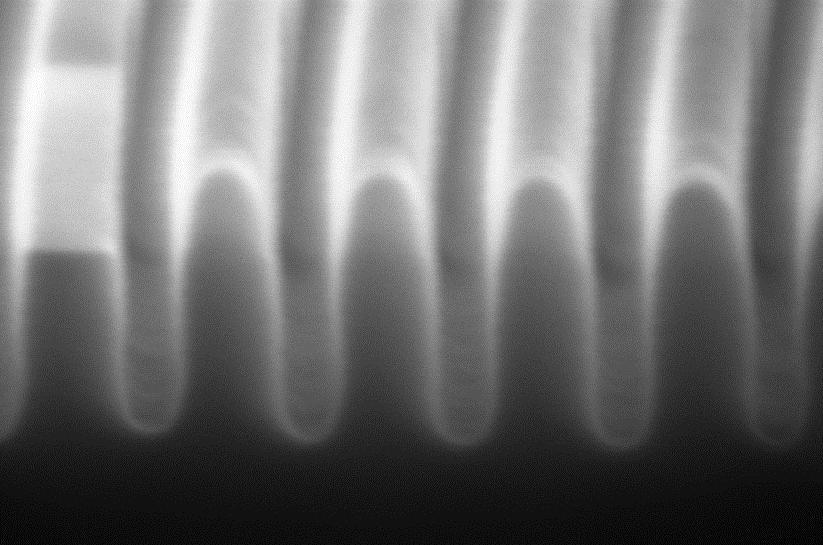
25nm wide Si trenches etched to 110nm depth by ALE,
HSQ mask still in place.

Atomic Layer Etching Systems

PlasmaPro 100 ALE

PlasmaPro 100 ALE

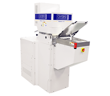
The PlasmaPro 100 ALE delivers precise process control of etching for next-generation semiconductor devices.

Specially designed for processes such as recess etching for GaN HEMT applications and nanoscale layer etching, the system's digital/cyclical etch process offers low damage, smooth surfaces.

Key Features

  • Digital/Cyclical etch process – etching equivalent of ALD
  • Low damage
  • Smooth etch surface
  • Superb etch depth control
  • Ideal for nanoscale layer etching (e.g. 2D Materials)
  • Wide range of processes and applications:
    • Low damage GaN HEMT recess etch for power electronics and RF devices
    • 2D materials patterning/thinning
    • Nanostructured SiO2, Si, SiN
    • III-V materials

Questions? Ask our experts today for more information.

CONTACT US

Applications for Atomic Scale Processing


Related Content