Part of the Oxford Instruments Group
Expand
Collapse
Part of the Oxford Instruments Group
Automatic Endpoint Detectors (EPDs) use process-integrated hardware to analyse what’s happening on the wafer and/or in the system chamber to interpret critical changes that require a process to end or move to the next process step.
There are two automatic EPD formats available from Oxford Instruments Plasma Technology’s Upgrades programme: Optical Emission Spectroscopy (OES) and Laser Interferometry (LI).
An OES endpoint detector kit typically consists of a spectrometer connected to a chamber viewport window via a fibre optic cable (see figure 1). The fibre optic cable then feeds data to a PC that is programmed to detect an endpoint signature (see figure 2).
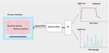
Figure 1. OES Endpoint set-up
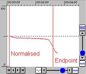
Figure 2. OES endpoint of photoresist removal
OES EPDs monitor the optical emissions from the whole plasma, measuring light intensity at various wavelengths in the chamber when a process is running. Relatively large open (etchable) areas are required when using OES EPD to control a wafer etch process, to maximise etch by-product concentrations, for a strong and measurable endpoint signal. When etching down to an underlying layer that requires a different chemistry to etch it, , OES EPD can be used to measure the drop in etch by-products during this transition and optimally stop the process to meet a etch depth specification.
OES EPDs can also provide advance warning of potential processing problems, as well as offering an understanding of what’s happening inside the chamber. For example, when using a plasma clean to remove by-products from the chamber walls, OES EPDs can be used to detect the point at which material on the sidewalls has been removed. Therefore OES EPDs can identify the optimum point at which the next wafer can be introduced into the chamber, or the point when the chamber is safe to open for maintenance when hazardous gasses have been used for processing. In-situ monitoring can also provide useful data on the health of the chamber and process, providing a broad visualisation of the overall processing environment.
Laser interferometry (LI) EPDs monitor the wafer directly by focusing a small laser spot (~20-60μm diameter and 670, 905, or 980nm wavelength) onto its surface and then measuring the reflected light intensity.
LI EPD kits typically consist of a special camera that’s mounted on top of the etch chamber (see figure 3), providing a TV image of the wafer surface, and then focusing a laser spot onto the wafer. The camera also collects the reflected laser light to provide a measure of the wafer reflectance. The spot can be positioned at a particular point on the wafer surface via movement of the camera’s x-y table. The laser spot is usually placed on an open area of the wafer, ideally >100x100μm near the centre of the wafer. LI has the additional benefit of being capable of measuring a point on full wafers and small samples (e.g. wafer pieces) and also etch depth within a transparent layer.
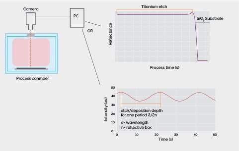
Figure 3. Laser Endpoint set-up
When LI is used in a production environment, a larger test area (up to 1x1mm) should be provided near the centre of the wafer. If a large test area is not provided, then manual positioning of the spot is required for each run, rendering automation impossible.
In summary, OES EPDs are typically used by customers seeking consistency in chamber conditions for optimum wafer-to-wafer repeatability and on-wafer analysis during processing, where there is a stop layer and sufficient open area for a strong signal. LI EPDs are typically used by customers seeking on-wafer etch depth accuracy, and automated LI EPD can be achieved when there is a centralised test area provided.
Both formats are suitable in a wide range of common semiconductor industry environments, including manufacturing and high-volume production, where accuracy and repeatability is paramount.
With manufacturers continuously striving for higher performance devices at smaller die sizes, there’s a constant demand to increase the consistency, quality, and longevity of devices. EPDs are an effective mechanism for achieving the advancements in consistency and uniformity that delivers higher device performance.
In multi-process production scenarios, increasing consistency in output for one process step allows manufacturers to also maintain stability in the potentially sensitive process steps that follow. Therefore EPDs can help deliver a continuous stream of consistency and repeatability throughout the device fabrication flow, allowing process steps to operate within their optimum process window.
We recently used EPDs to help a long-standing production customer solve a process problem and expand production capacity.
Our customer wanted to expand capacity in one of its established device fabrication lines by purchasing additional systems. Several years had elapsed since our customer’s last system purchase, meaning the design of our newer systems had evolved to embrace more advanced technology and components, as well as a more intuitive user interface. However, the on-wafer result that the new equipment produced had to precisely match the older equipment’s results to complement our customer’s other upstream and downstream production processes. This was a challenge because the time gap between purchasing the existing and new equipment was significant.
The critical process to be transferred from our customer’s existing equipment to the new equipment was a very sensitive shallow etch with short process time. This form of transfer presents one of toughest challenges for matching system performance in new and old equipment.
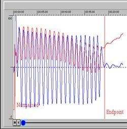
Figure 4. Graphic of Endpoint monitoring of wafer
However, LI EPD was effective because it can overcome variations in incoming material, ambient lab conditions, slight variations in mask consistency, first wafer effect, and in this case, some subtle system differences, to deliver the same consistent on-wafer result. LI EPD measures the progress of the etch in real time, on the wafer surface, and then automatically adjusts process time to end the process precisely and at the required depth. The endpoint system therefore compensates for small variations in either the materials or system that can speed-up or slow-down the expected etch rate.
A well-known phenomenon when running batches of wafers involves a slightly slower etch rate on the first wafer, because the chamber starts from ‘standby’ (this phenomenon is known as the “first wafer effect”). Whilst the chamber might be process-ready in ‘standby’ mode, it is probably slightly cooler than it would be after the second or third wafer in a batch. As the batch run proceeds, the exothermic (heat producing) etch process warms the chamber, stabilizing by around the second wafer, depending on the process duration. Shorter process durations, typically used for shallow tight specification etches, exaggerates first wafer effect. For short duration etches, first wafer effect may increase or decrease etch rate for several wafers, so it may take 4-5 wafers in a batch before the chamber etch rate stabilises. Laser interferometry EPD monitors the progress of the etch and ends the process only when the target etch depth is reached by extending or shortening the process time to account for first wafer effect, system differences, or incoming material variations that might alter the etch rate.
Figure 4 below shows a typical example of a batch process where the etch depth has been controlled by endpoint:
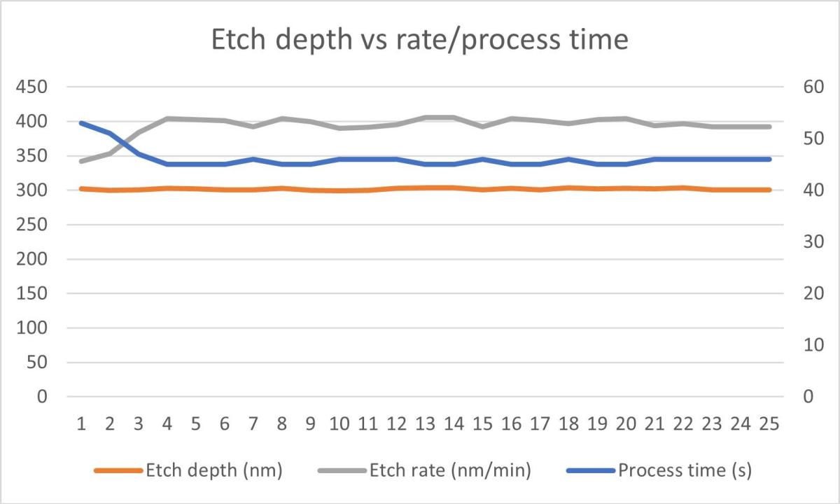
Figure 4. Etch depth vs rate/process time
Our expertise and commitment to solving technical challenges means we can help our customers increase quality and throughput. Our LI EPDs have proven successful in solving a challenging situation involving the fabrication of devices in GaN MISHEMT. This device requires a very shallow and highly-depth critical recess formation to achieve optimal device performance characteristics. An LI EPD solution was identified by our technical team, which then worked in collaboration with customers and external partners to address the challenges of GaN MISHEMT fabrication. In this example, the addition of LI EPD helped solve the sensitive processing challenge that subsequently led to the device design being realised. To achieve this, we utilised atomic layer etch, with LI EPD, delivering the desired etch quality and depth to a target etch depth accuracy of ±0.5nm. This suite of GaN processing techniques, integrated seamlessly onto a single platform, has since been adopted by several leading power device manufacturers in Japan and USA.
With endpoint detectors consistently featuring amongst our most popular upgrade packages over several years, there are many other specific examples of OES and LI endpoint detection adding real value to our customers operations. It’s also notable that in recent times, there’s been a significant upsurge in customer interest for our plasma atomic layer deposition (ALD) and atomic layer etch (ALE) modules in quantum, microLEDs, GaN power and many other research and manufacturing applications, all of which are often enabled by EPD techniques.
Figure 5. Horiba Laser Endpoint Detector
Table 1 below shows some typical criteria and table 2 shows a guide for applications.
Table 1. Typical criteria for the endpoint techniques.
| Property | OES | Laser |
| Sample Size | Large samples, wafers and chamber | Any wafer sample (not applicable for chamber analysis) |
| Endpoint detection area | Whole plasma | Localized detection at spot |
| Endpoint type | Only layer transitions and chamber condition | Transitions or etch depth in-layer |
| Pattern requirements | Any size/shape/location, if total exposed area is sufficient | >100x100μm needed close to the centre of the wafer for manual spot positioning |
| Operation | Fully automated | Manual spot positioning, unless a much larger test area is provided |
Table 2. Typical applications for the endpoint techniques.
| Application | OES | Laser |
| Chamber cleaning | ✓ | x |
| In-layer depth targeting | x | ✓ |
| Complex multilayers (e.g. metal/oxides, III-V) | ✓ | ✓ |
| Dielectric thin film removal | ✓ | ✓ |
| Metal thin film removal | ✓ | ✓ |
| Failure Analysis | Large samples only | ✓ |
| SOI Endpoint | ARDE effects | ARDE effects |
| Plasma analysis/chamber condition monitoring | ✓ | x |
For a free system review, more information and pricing, please contact your local customer service sales support team now. Or visit the upgrades area of our website https://plasma.oxinst.com/service-support/upgrades/endpoint-detectors.

Kurt Perry
Technical Content Specialist at Oxford Instruments Plasma Technology


© Oxford Instruments 2026