Part of the Oxford Instruments Group
Expand

Atomic scale processing (ASP)

Wafer-scale processing with control at the atomic scale

PlasmaPro ASP

Delivers a step-change in capability with rapid, high-rate deposition of conformal, tunable oxides and nitrides

Atomic scale processing (ASP)

Atomic Scale Processing (ASP) means wafer-scale processing with control at the atomic scale. This atomic-level control extends to deposition of thin films, removal or etching of material, and growth of 1D and 2D materials with their distinctive unique properties such as graphene.

Our range of plasma processing systems provides a complete solution to Atomic Scale Processing. We provide unique cluster capability or stand alone systems enabling the manipulation of matter with atomic scale precision on a production scale.

  • 1D & 2D materials growth - Chemical vapour deposition (CVD) & ALD of atomically thin structures

Request information
Download brochure

ALD overview


ALD of dielectrics

ALD of dielectrics, nitrides and metals with low damage. Our unique cluster capability provides the ability to cover surfaces directly without exposure to air. For instance these could be etched interfaces or freshly grown 2D materials such as MoS2 or graphene covered by ALD dielectrics or capping layers which can be a big advantage for a wide range of devices.

ALD of dielectrics & metals with low damage

CVD overview


CVD & ALD of atomically thin structures: 1D and 2D materials.

Unique devices can be constructed by covering nanowires with ALD films or etching 1D and 2D materials to tune their properties.

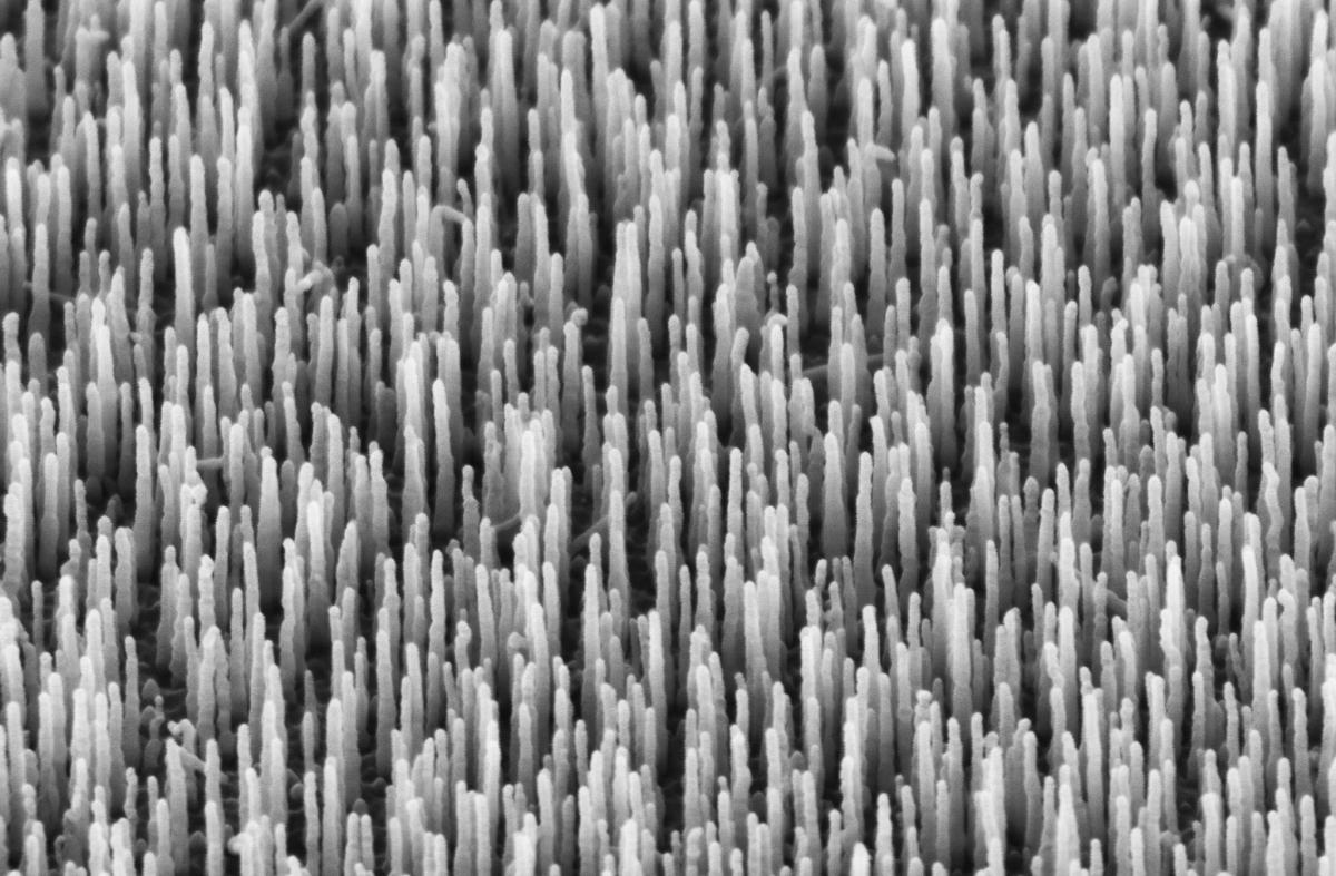
CVD growth of ZnO nanowires using DEZn precursors.
(Courtesy of Nanoscience Centre, Univ. of Cambridge)
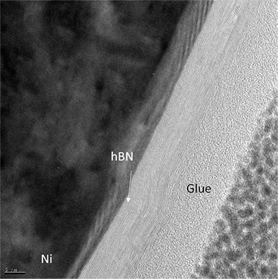
CVD growth of hBN

ALE overview


ALE of Silicon, GaN & 2D materials. As these materials perform essential functions in a wide range of devices, our ability to etch these with extreme control and low damage can be an enabling technology. Furthermore combining ALE with deposition and growth will provide unique advantages in your device making.

Featured ASP products

PlasmaPro ASP

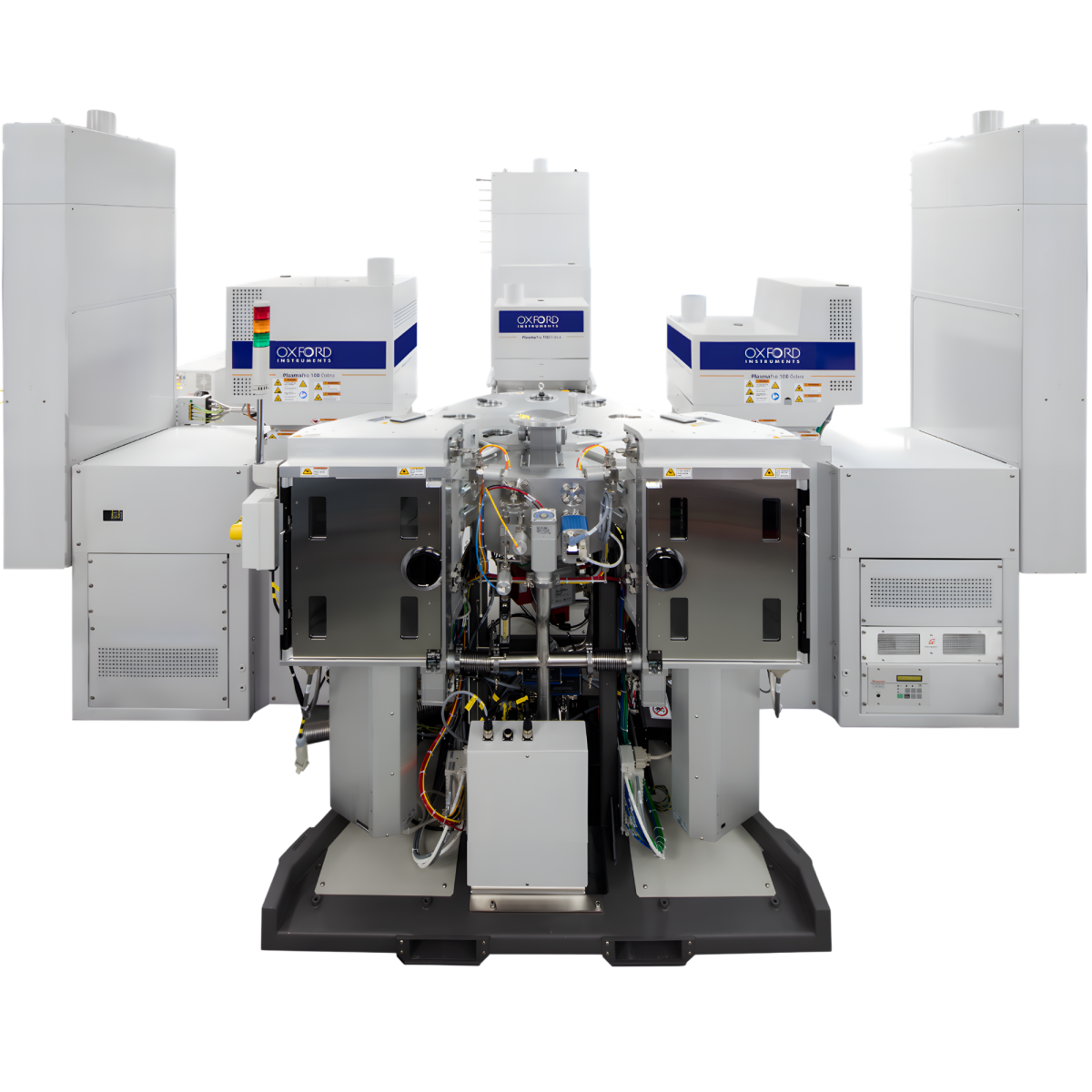
Based on production-proven platform for corporate/specialised R&D, PlasmaPro ASP has been designed to ensure high quality materials that can be deposited at speed with flexibility to run multiple chemistries to give excellent layers for incorporation into devices. Our cutting-edge plasma enhanced ALD (PEALD) system offers flexibility, conformality, and tunability of ALD with speed for higher throughput and thicker films.

  • Faster than conventional remote plasma

  • Reduced precursor consumption which is beneficial for the environment and cost of running
  • High material quality
  • Low cost of ownership

  • Improved serviceability and maintenance

  • Low volume chamber for speed

  • Low substrate damage

  • Higher process stability


Request information
Download brochure

PlasmaPro ASP overview


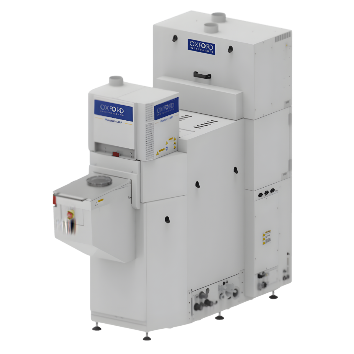
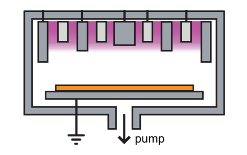
PlasmaPro ASP has shared platform with Atomfab to deliver fast and low damage remote PEALD. Remote PEALD offers superior device performance compared to thermal ALD and direct plasma ALD. It is compact to limit the effective chamber volume for rapid gas exchange and it is effective over the full 200 mm wafer diameter.​

PlasmaPro ASP features


  • High speed remote plasma source
    - High and uniform radical density and low ion energies for low damage, fast saturation
    - PLC and AMU control allows rapid striking
  • Excellent precursor and process control
    - Up to 6 precursors, bubbled or vapour drawn
  • Wafer electrode
    - 200 mm wafer electrode with bias
    - Up to 400 °C deposition temp.
    - 200 °C heated inner chamber
  • Control system
    - Ease of service and simplified wiring
    - Improved diagnostics for service
    - No separate ‘electronics’ rack
  • Ease of cleaning
    - Removable metal surfaces in chamber
    - Purged outer chamber and lower pumping areas

PlasmaPro ASP applications


  • Low damage GaN HEMT passivation for power electronics and RF devices
    • Low-oxygen content conductive nitrides with all-metal plasma source enabling fast cycle times, suitable for quantum devices
    • Low damage graphene encapsulation for datacom applications

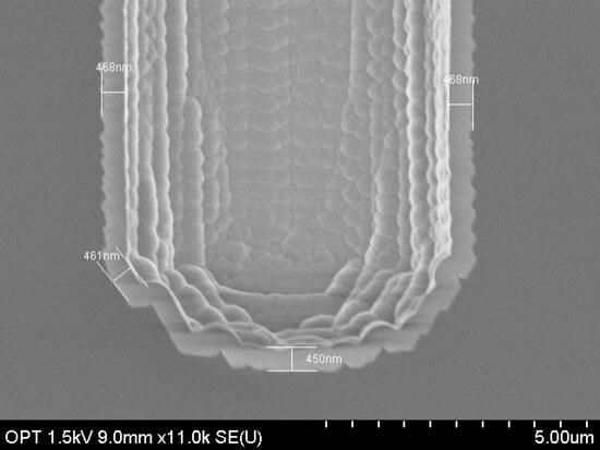
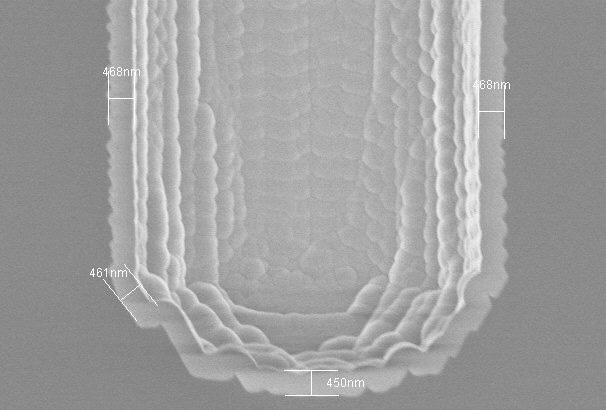
    450 nm conformal SiO2 deposited in 32:1 aspect ratio trench using PlasmaPro ASP.

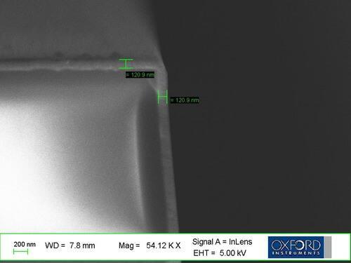
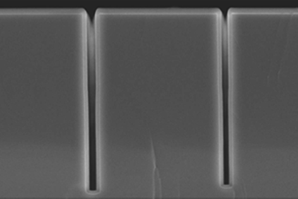
    130 nm conformal superconducting NbN deposited in 8:1 aspect ratio trench using PlasmaPro ASP.

    PlasmaPro ASP specifications


    Specifications

    PlasmaPro ASP

    Precursor lines

    Maximum 6 (any combination)​

    Precursor size (ml)

    200

    Precursor type

    • Vapour draw - cooled ​
    • Vapour draw - heated ​
    • Bubbled – heated

    Handling

    Loadlock

    Gas pod

    4 Process + 1 Ar (onboard) ​

    Electrode

    400 °C grounded/ biased

    Roughing pump

    600 m3/hr

    Compliance

    UL Standard, designed for SEM 2S

    Software

    PTIQ

    PEALD process library

    Al2O3, SiO2, NbN, TiN, more in development

    Request information
    Download brochure

    PlasmaPro 100 ALE

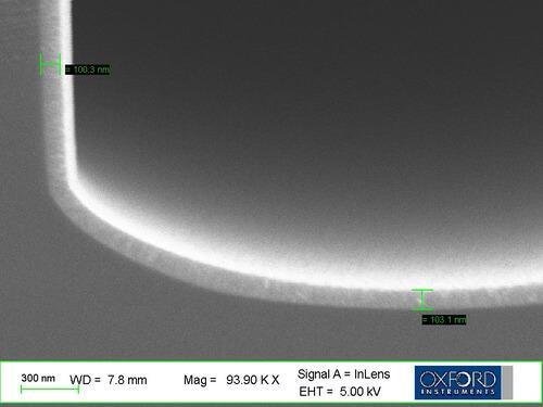
    The PlasmaPro 100 ALE delivers precise process control of etching for next-generation semiconductor devices. Specially designed for processes such as recess etching for GaN HEMT applications and nanoscale layer etching, the system's digital/cyclical etch process offers low damage, smooth surfaces.

    • Digital/cyclical etch process – etching equivalent of ALD
    • Low damage
    • Smooth etch surface
    • Superb etch depth control
    • Ideal for nanoscale layer etching (e.g. 2D materials)
    • Wide range of processes and applications
    Request information
    Download brochure

    Key features of PlasmaPro 100 ALE

    As layers become thinner to enable the next-generation semiconductor devices, there is a need for ever more precise process control to create and manipulate these layers. The PlasmaPro 100 ALE delivers this by enhancing our Cobra ICP platform with specialised hardware for atomic layer etching.

    • Delivers reactive species to the substrate, with a uniform high conductance path through the chamber - Allows a high gas flow to be used while maintaining low pressure
    • Variable height electrode - Utilises the 3-dimensional characteristics of the plasma and accommodate substrates up to 10 mm thick at optimum height
    • Wide temperature range electrode (-150 °C to +400 °C) which can be cooled by liquid nitrogen, a fluid re-circulating chiller or resistively heated - An optional blow out and fluid exchange unit can automate the process of switching modes
    • A fluid controlled electrode fed by a re-circulating chiller unit - Excellent substrate temperature control
    • RF powered showerhead with optimised gas delivery - Provides uniform plasma processing with LF/RF switching allowing precise control of film stress
    • ICP source sizes of 65 mm, 180 mm, 300 mm - Delivers process uniformity up to 200 mm wafers
    • High pumping capacity - Gives wide process pressure window
    • Wafer clamping with He backside cooling - Optimum wafer temperature control

    Applications for PlasmaPro 100 ALE

    • Low damage p-GaN HEMTs and recessed gate MISHEMTs etch for power electronics and RF devices
    • 2D materials patterning/thinning
    • Nanostructured SiO2, Si, SiN
    • III-V materials
    • Solid-state lasers InP etch
    • VCSEL GaAs/AlGaAs etch
    • Hard mask deposition and etch for high brightness LED production
    • SiO2 and quartz etch
    Request information
    Download brochure

    Atomfab 

    Atomfab is the fastest remote plasma production ALD system on the market

    Solutions for your productions needs:

    • Competitive CoO
    • Quick, easy maintenance
    • Excellent film uniformity
    • High material quality
    • Low substrate damage
    • Faster cycles times, high throughput
    • Clusterable and automated wafer handling
    Request information
    Download brochure

    Atomfab benefits


    Atomfab's ALD technology offers precisely controlled ultra‑thin films for advanced applications on the nanometre scale, with conformal coating of sensitive substrate structures.

    Process benefits for passivation of power and RF devices

    • Guaranteed processes setup by our engineers
    • Lifetime process support for additional/new processes
    • Low-damage plasma processing
    • High quality deposition with low film contamination
    • Low particle levels
    • Short plasma exposure times enabling high throughput
    • Plasma surface pre-treatments

    Advantages of plasma ALD for GaN, power and RF devices

    • With plasma pre-treatment prior to deposition to enhance interface quality
    • Low damage, uniform deposition
    • Remote plasma ALD with controlled ion energy from near zero to 30 eV
    • ALD passivation, gate dielectric by Al2O3 films.

    Read more about how ALD can optimise GaN power devices in our white paper.

    Atomfab features


    Revolutionary plasma source: Atomfab system uses a patent pending remote source specifically designed for atomic scale processing.

    • Low damage for sensitive substrates for maximum device performance
    • Fast cycle times and reliablity with uniform plasma exposure and film deposition
    • Short plasma times (250 ms) enabled by patent-pending AMU
    • Short strike time (80 ms) for high throughput
    • Reproducible strike time and low reflected power for high yield

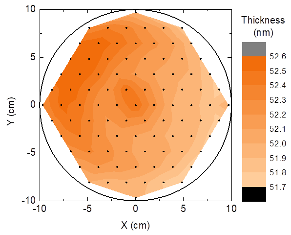
    Plasma ALD Al2O3 at 300 °C

    Specification

    Within wafer thickness uniformity

    <±1.0%

    Wafer-to-wafer thickness repeatability

    <±1.0%

    Breakdown voltage

    ≥7.0 MV/cm

    Global customer support

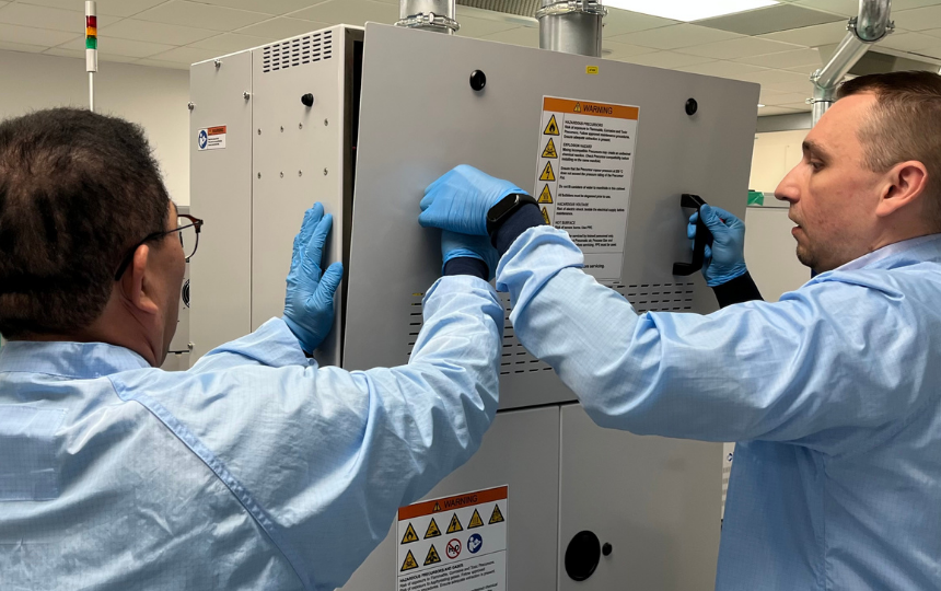
    Oxford Instruments is committed to providing a comprehensive, flexible and reliable global customer support. We offer excellent quality service throughout the life of your system.

    • Remote diagnostics software provides quick and easy fault diagnosis and resolution.
    • Support contracts are available to suit the budget and situation.
    • Global spares in strategic locations for quick response.
    Find out more

    NEW: PTIQ software

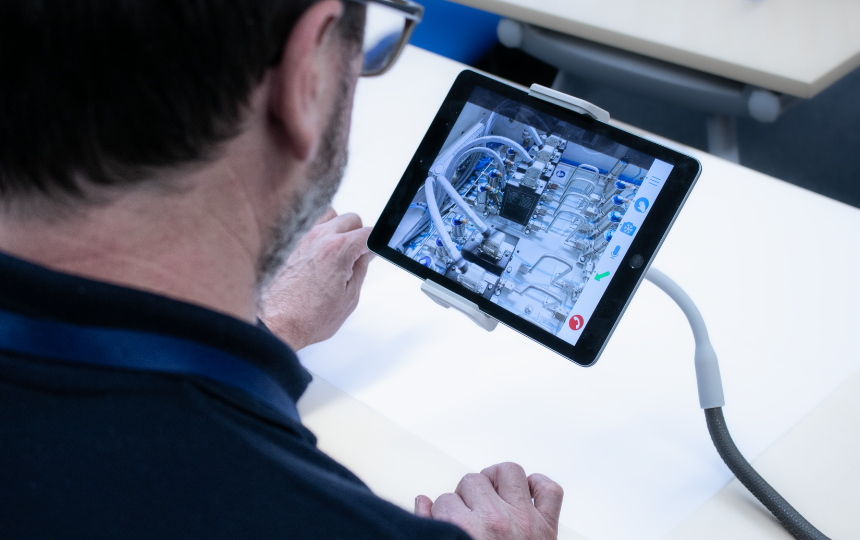
    PTIQ is the latest intelligent software solution for PlasmaPro and Ionfab processing equipment.

    • Exceptional level of responsive system control
    • Optimise system and process performance
    • Different levels of software to suit your requirements
    • Brand new intuitive layout and design
    Find out more

    Explore our comprehensive technical training courses

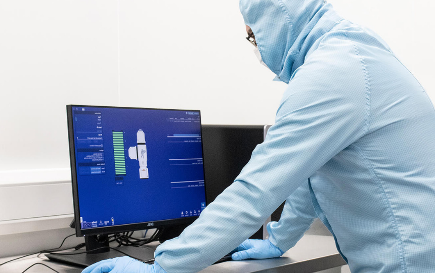
    At Oxford Instruments Plasma Technology, we offer a wide range of technical training courses designed to suit all skill levels and needs.

    • Level 1 (Introductory): New system users for all platforms
    • Level 2 (Intermediate): Equipment and maintenance training for all platforms
    • Level 3 (Advanced): for plasma etch and deposition, ion beam and PEALD systems
    • Specialist technical modules: process and handler technical training for all platforms
    Find out more

    Latest news

    Upcoming events