Part of the Oxford Instruments Group
Expand

Ionfab Ion Beam

Ionfab serves a diverse set of ion beam etch (IBE) and deposition (IBD) process requirements across a wide range of applications.

  • Single wafer or cluster wafer handling
  • Multiple mode functionality
  • Capable of clustering with other plasma systems
  • Dual-beam configuration
  • Very low surface film roughness
  • Unmatched batch uniformity
DOWNLOAD BROCHURE
REQUEST PRICING

Unique technology serving multiple applications

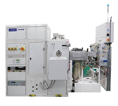
Ion beam technology provides an exceptionally versatile approach to etch and deposition by offering a single tool and maximising system utilisation.


Ion Beam Etching

  • Slanted etching
  • Laser facet etching
  • Magnetoresistive random access memory (MRAM)
  • Dielectric films
  • III-V photonics etching
  • Spintronics
  • Metal contact and track
  • Superconductors

Ion Beam Deposition

  • Laser facet coating including high- and anti-reflection
  • Ring laser gyroscope mirrors
  • X-ray optics
  • II-VI based infrared sensors
  • Infrared sensors (Vanadium oxide, II-VI)
  • Telecom filters

High quality Ion Beam Etching

Superior process repeatability and low cost of ownership make the Ionfab tool an excellent system that is configurable from R&D to batch production.

Key Benefits

  • Flexible configuration for advanced research applications
  • Unmatched uniformity and process reproducibility for production
  • Flexible wafer handling capability – single wafer load lock or cassette-to-cassette robotic handler

Etching Modes

  • Ion Beam Etching (IBE) / Ion Beam Milling
  • Reactive Ion Beam Etching (RIBE)
  • Chemically-assisted Ion Beam Etching (CAIBE)

Hardware Features

Ion Etching Source 150mm or 300mm for up to 4" and 8" respectively
Etching Area Up to 200mm diameter or 150mm square
Platen Speed Up to 20rpm
Platen Tilt Angle 0º to 75º between beam and normal to substrate surface
Platen Heat Embedded heaters up to 300ºC with PID controln
Platen Cooling Fluid coolant 5ºC to 60ºC with He or Ar backside gas for substrate cooling (up to 50Torr) 
IBE processing chamber schematic


Etch Ion Sources

  • Three-grid assembly designs
  • Grid designs tailored for specific etch requirements
  • Filamentless DC plasma bridge neutraliser (PBN) for low maintenance

DOWNLOAD BROCHURE

High quality Ion Beam Deposition

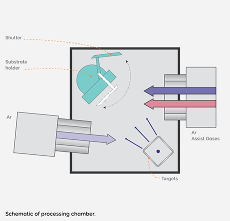
High vacuum operation allows Ion Beam Deposition to deliver thin films with high quality and excellent electrical and optical properties.

Key Benefits

  • High quality thin films with ultra-low contamination
  • High throughput with reduced footprint for lowest cost of operation
  • Unmatched batch uniformity and process reproducibility
  • Very accurate optical film thickness control
  • Very low surface film roughness

Deposition Modes

  • Ion Beam Sputter Deposition (IBSD)
  • Ion-assisted Sputter Deposition (IASD)
  • Reactive Ion Beam Deposition (RIBD)

Hardware Features

Ion deposition source  150mm
Deposited area Up to 200mm
Substrate rotation speed Up to 20 RPM
Number of targets Up to 4 targets
Platen size  Up to 8 inch wafer
Platen rotation Up to 500rpm
Platen tilt angle  0º to 75º between beam and normal to substrate surface
IBD processing chamber schematic


Deposition Key Features

  • Multiple targets with rotating shutter
  • Wide range of sputter target sizes with matching deposition ion source grid designs
  • Optional rotating and tiltable high speed substrate holder

DOWNLOAD BROCHURE

Superior performance in key applications

Augmented Reality Optical Combiners

  • Solution for etching surface-relief gratings for waveguide combiners on large processing area
  • Angled SiO2 grating using Ion Beam Etching (IBE) for precise angle control
  • Uniform angle control over 200 mm wafer size
  • Patent-filed solution to enable high-yield manufacturing

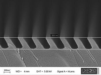
We have many years of expertise in etching the slanted feature on large areas. Our solutions are designed to deliver the manufacturing quality required for surface-relief gratings.

Our solution delivers market-leading uniformity for wafer sizes up to 200mm.

DISCOVER OUR AR SOLUTIONS >

Edge-emitting Lasers

  • Laser facet etching with option of angled facet etch for control over laser beam emission angle
  • High quality laser facet coating for high power laser
Laser image

Infrared Sensors

  • Good resistance repeatability for VOx film
  • Temperature coefficience of resistance shows no hysterisis
IR image

Global Customer Support

Oxford Instruments is committed to providing a comprehensive, flexible and reliable global customer support. We offer excellent quality service throughout the life of your system.

  • Remote diagnostics software provides quick and easy fault diagnosis and resolution
  • Support contracts are available to suit the budget and situation
  • Global spares in strategic locations for quick response

Contact Us Today For More Information

Speak to our experts or request pricing information today.


Related Content