 Part of the Oxford Instruments Group
Expand
Collapse
Part of the Oxford Instruments Group
Following our recent discussion on plasma enhanced ALD for superconducting materials, here we turn our attention to a very different, but equally challenging, materials system: high-κ dielectrics on graphene.
Graphene has long been regarded as a wonder material for electronic and optoelectronic applications due to its exceptional electrical, thermal, and mechanical properties. However, one key challenge has continued to limit its large-scale adoption: how to deposit very thin, high-quality dielectric layers without damaging its atomically thin lattice. Such integration is essential for graphene-based electronic and optoelectronic devices requiring a low equivalent oxide thickness (EOT), such as high-speed optical modulators for next-generation data communication systems.
As discussed in our recent blog on plasma enhanced ALD for superconducting TiN, ALD (atomic layer deposition) is valued for its excellent uniformity, conformality, and thickness control. However, when applied to 2D materials such as graphene, its fundamental growth mechanism encounters a unique challenge.
Conventional ALD relies on chemisorption to surface sites to initiate nucleation and sustain uniform growth. In contrast, 2D materials are atomically thin, chemically inert and lack out-of-plane reactive groups. Their pristine basal planes therefore provide very few reactive sites for ALD precursors, leading to delayed nucleation, island formation or incomplete film closure.
While plasma enhanced ALD (PEALD) can help activate surfaces and improve film quality, direct plasma exposure introduces an additional risk: energetic species can disrupt the atomic lattice of 2D materials. This intrinsic trade-off between nucleation, film quality, and material integrity has made the deposition of high-quality dielectrics on 2D materials a long-standing challenge.
Over the years, Oxford Instruments ALD tools have been used to explore multiple approaches for depositing high-quality dielectrics on 2D materials. Thermal ALD can deliver excellent film quality with minimal damage to graphene but may need difficult-to-scale seeding approaches to get thin closed layers, and typically needs high temperatures to get good film quality. Our PEALD approach, which we focus on here, offers a scalable fast seeding approach which enables ultra-thin, high-quality films. Together, these methods highlight the versatility of ALD on Oxford Instruments systems, allowing researchers to select the approach best suited to their device and application requirements since both thermal and plasma ALD, and combinations thereof, can be done on our systems.
We developed a two-step PEALD process (patent #GB2613821B) that protects graphene while enabling high-quality dielectric growth.
Step 1: Protective layer
A very thin non-stoichiometric aluminum oxide (AlOX) layer is applied to the graphene. It shields the graphene while helping the next layer to grow evenly.
Step 2: Dielectric growth
A high-quality dielectric is added on top without exposing the graphene to harmful plasma. The protective layer absorbs most of the plasma energy, keeping the graphene intact.
All steps were performed on the Oxford Instruments Atomfab™ PEALD system, achieving excellent uniformity across the wafer.
Full details: https://doi.org/10.1016/j.mssp.2025.109829 [1]
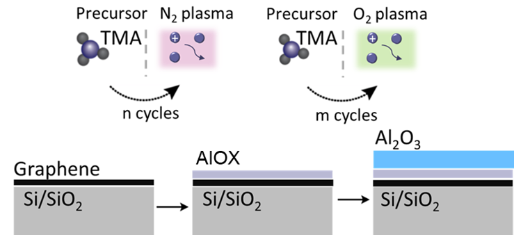
Figure 1: Schematic of the fully in situ PEALD process used to deposit AlOX/Al2O3 dielectrics. A thin AlOX layer is first deposited on the wafer using trimethylaluminum (TMA) and N₂ plasma, providing effective protection of graphene. This is followed by Al₂O₃ deposition using TMA and O₂ plasma.
To verify that graphene remained undamaged throughout the process, Raman spectroscopy was performed using a WITec Raman microscope, another Oxford Instruments tool.
The appearance of the D peak is a well-known indicator of defects in graphene. While direct oxygen plasma exposure produces a pronounced D peak, samples protected by the AlOX layer show a strong suppression of the D peak and a sharp, well-defined 2D peak, confirming preservation of graphene’s crystalline structure.
Having both the Atomfab™ and WITec systems in-house enabled a rapid, iterative workflow. This involved depositing, characterising, and refining, and reduced optimisation cycles from days, or even weeks, to hours.
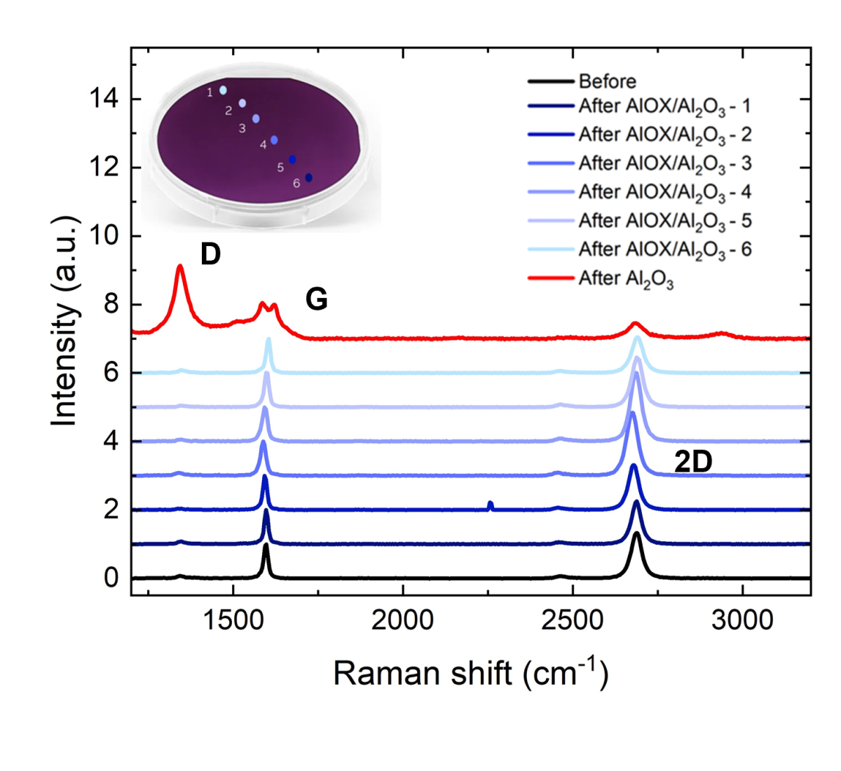
Figure 2: Raman spectra of graphene before and after encapsulation. The AlOX interlayer, deposited using low-dose remote nitrogen plasma, leaves the D peak unchanged, indicating that the graphene remains undamaged during subsequent processing. Red line indicates Al₂O₃ without AlOX encapsulation.
To demonstrate device relevance, top-gated graphene field-effect transistors (GFETs) were fabricated using the AlOX/Al2O3 dielectric stack. Devices across multiple dies exhibited:
Prior to dielectric deposition, the charge neutrality point (VDirac) lay outside the measurement window; following encapsulation, it shifted back into range, indicating high-quality graphene encapsulation. This encapsulation results in enhanced carrier mobility by reducing phonon and Coulomb scattering and by limiting the adsorption of water and oxygen molecules on the graphene surface.
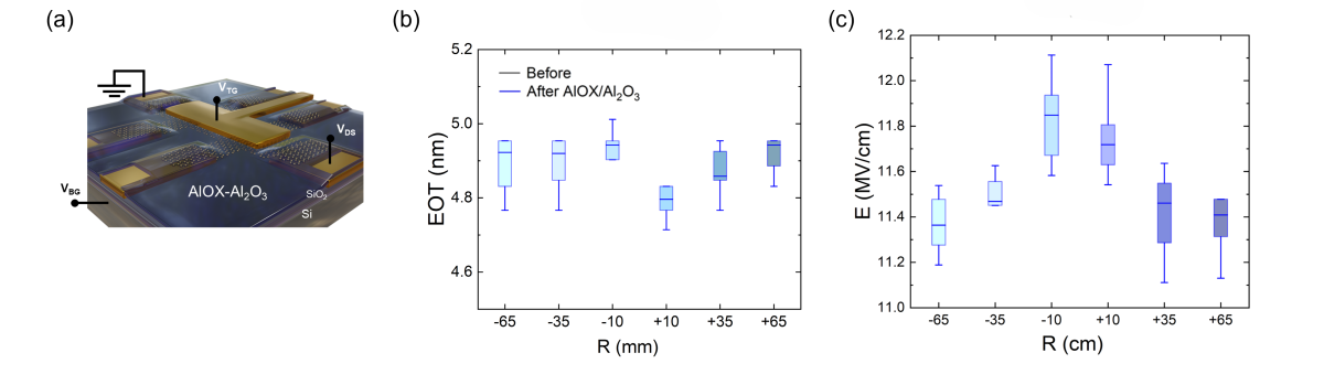
Figure 3: (a) Two-point double-gated GFET with bottom source/drain contacts and an AlOX/Al2O3 dielectric stack. Wafer-scale statistics of (b) EOT and (c) E from double-gate measurements.
This process addresses one of the biggest obstacles to integrating graphene with industrial electronics: depositing high-quality dielectrics at scale without introducing defects.
By combining AtomfabTM’s precise deposition control with WITec’s rapid, high-resolution Raman characterisation, we demonstrate a reproducible process that preserves graphene quality while enabling high-performance electronic devices.
Future work will focus on understanding the atomic-scale growth mechanism of AlOX on graphene and extending this protective-layer strategy to other 2D materials such as, 2D transition metal dichalcogenides (TMDs) MoS2 and WS2. Ultimately, this approach opens a pathway toward scalable integration of ultrathin dielectrics in 2D electronic and optoelectronic devices.
Each step brings us closer to bridging the gap between laboratory demonstrations and industrial scale 2D material technologies.
We developed this process, and its integration into devices in collaboration with AMO GmbH via the 2D-Pilot Line, part of the Graphene Flagship.
To discover whether Oxford Instruments can support and develop your application, please get in touch with our team and we will be happy to discuss how our tools can benefit you.
Ask a questionFollow our publications page to see what our customers and our researchers at Plasma Technology are doing with our systems.
Keep in touch with our Oxford Instruments Semiconductors page on LinkedIn to find out what conferences you can speak to us at and all of our latest updates.
1. S. Riazimehr et al., “Plasma-enhanced atomic layer deposition of Al2O3 on graphene via an in situ-deposited interlayer,” Mater. Sci. Semicond. Process., vol. 199, p. 109829, Nov. 2025, doi: 10.1016/j.mssp.2025.109829.

Researcher in Residence Applications
Sarah holds a PhD in electronics with a focus on 2D materials from RWTH Aachen University. She developed a strong background in semiconductor processing through her academic and industrial work at KTH Royal Institute of Technology, RWTH Aachen University, and Micronit Microtechnologies.
She subsequently joined Oxford Instruments, where she focuses on 2D devices, interface engineering, and dielectric deposition.


© Oxford Instruments 2026

