 Part of the Oxford Instruments Group
Expand
Collapse
Part of the Oxford Instruments Group
Welcome back to our blog from Oxford Instruments Plasma Technology!
With the return of our blog page, we wanted to share our latest results on plasma enhanced atomic layer deposition (ALD) of superconducting TiN. Using our high-throughput PlasmaPro ASP platform, critical temperatures of > 4.3 K were achieved for TiN films. But first…
Plasma enhanced ALD has become an established technique for depositing material both in high volume manufacturing (HVM), and in smaller scale industrial and academic research applications. The interest in ALD is driven by the high material quality that can be achieved, coupled with the conformality, uniformity and thickness control that are typically observed. When thinking of ALD, many will think of thermal ALD, but at Oxford Instruments, we have over 40 years of experience in plasma physics, making systems which can provide our customers with both thermal ALD and the extra benefits of plasma enhanced ALD.
Benefits of ALD: |
Benefits of plasma enhanced ALD: |
Thickness control at the nm-scale and below simply by varying the number of ALD cycles |
Substrate biasing to control the incident ion energy and tune material properties for your application |
Uniformity at the wafer scale due to self-limiting half-cycles |
Lower deposition temperatures by utilising the enhanced reactivity of plasma radicals |
Conformal material deposition on complex 3D structures |
Shorter purge times due to lower residence times of co-reactants |
To find out more about our ALD solutions, click here:
Superconducting materials are vital for the future of quantum computing with various superconducting materials used in the fabrication of superconducting quantum devices and qubits. Titanium nitride (TiN) is a material used for many applications and is of particular interest in quantum devices due to its tuneable superconducting properties, chemical stability and compatibility with HVM.
Our Oxford Instruments PlasmaPro ASP system provides high-throughput TiN deposition combined with excellent control of material properties, which can be applied to facilitate the fabrication of next generation quantum devices.
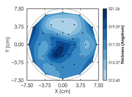
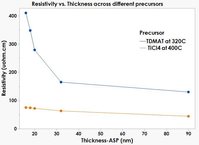
Figure 1: (a) Uniformity map for plasma ALD of TiN on a 6-inch (150 mm) wafer. (b) Resistivity as a function of film thickness comparing tetrakis(dimethylamido)titanium (TDMAT) and titanium tetrachloride (TiCl4) deposited at 320 ˚C and 400 ˚C, respectively. For applications where a low substrate temperature is required TDMAT could be preferred, while for the low resistivity TiCl4 would be best.
TiN films deposited on the PlasmaPro ASP can achieve resistivities as low as 60 µΩ cm for films >50 nm. These low resistivities are made possible by optimising process parameters to tune materials properties such as crystallinity and contaminant concentration, among other properties. Furthermore, the innovative chamber design we have developed facilitates faster ALD cycle times than typically seen for ALD of conductive nitrides. (1) Higher throughput means more experiments (wafers) per day, perfect for exploring a large parameter space and finding the best films for your research.
One specific quantum application where TiN is being explored is as a superconducting coating for through silicon vias (TSVs). Current superconducting TSVs rely on sputter deposition or chemical vapour deposition (CVD) to coat TSVs with superconducting materials, techniques which can struggle to conformally coat high aspect ratio (AR) structures. This has necessitated the use of sloped sidewalls to enable full coverage of the TSV. CVD coverage can be <50 % for features sizes with AR >10:1, requiring excess material deposition to ensure sufficient coverage throughout the TSV. (2) As superconducting quantum computing looks to advance to more complex chip designs and route signals between chiplets, denser TSV layouts will be required i.e. vias with vertical sidewalls and higher AR. As shown in Figure 2, plasma ALD can achieve the desired conformality, with >75 % film thickness at the bottom of the feature compared to the top for a 10:1 AR feature with one deposition. This minimises the amount of over deposition required and provides a more uniform film thickness throughout the device.
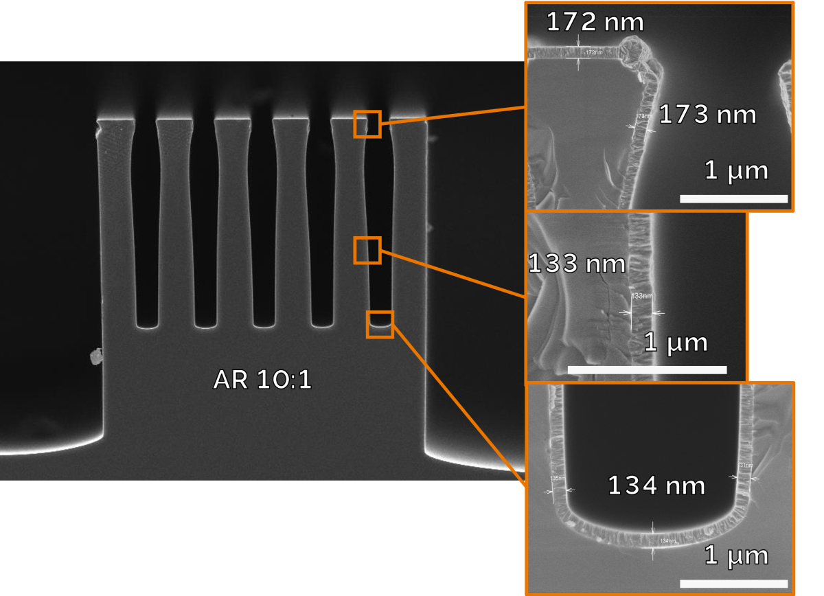
Figure 2: Si test structure for measuring conformality of ALD films. The TiN film is observed to fully cover the Si trench, with >75 % coverage ((Tbottom/Ttop)*100). In the zoomed in images on the right the crystalline nature of the TiN film can be seen. Error in recorded film thickness is ± 3 nm for the films measured with SEM.
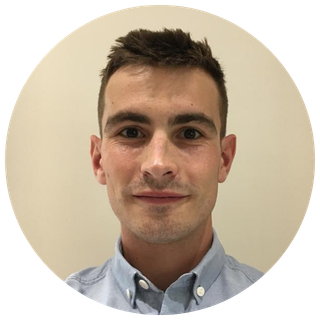
To confirm the utility of our plasma ALD TiN for quantum applications, superconducting transition temperature (Tc) measurements were obtained. This testing was done in collaboration with Oxford Nanoscience (now trading as Quantum Design Oxford) on a TeslatronPT Plus system, which allowed for two samples to be simultaneously cooled down and measured. Sample 1 had a Tc = 4.583 ± 0.002 K, and Sample 2 showed a similar result, with Tc = 4.700 ± 0.002 K, for both films a transition width of 0.007 ± 0.003 K was measured. The data for Sample 2 can be seen in Figure 3. The narrow transition width and high Tc, combined with good residual resistivity ratios of 1.27 and 1.37 for sample 1 & 2, respectively, are indicators of a high-quality TiN film with minimal contamination. The planar data presented here is indicative or how the TiN film would perform in planar circuit elements such as resonators, or in devices like Superconducting Nanowire Single Photon Detectors (SNSPDs).
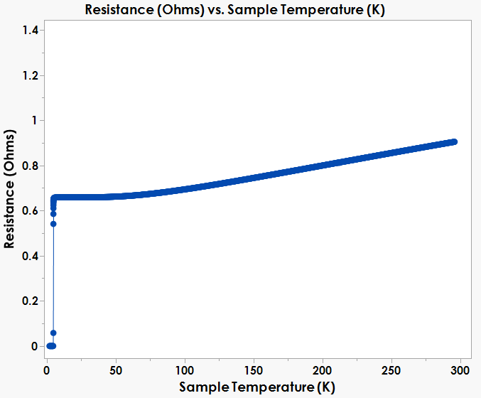
Figure 3: Resistance as a function of temperature for Sample 2 (film thickness 95 ± 5 nm) measured on a Quantum Design Oxford TeslatronPT Plus system. (a) Shows the full temperature range while (b) is a zoom in at the Tc to highlight the narrow transition width. Measurements were performed with an excitation current of 0.2 mA.
Plasma enhanced ALD is a powerful technique for depositing uniform, high-quality material on challenging 3D structures. The high Tc that can be achieved on our PlasmaPro ASP systems shows that plasma enhanced ALD is a viable processing technique for superconducting applications, such as quantum computing and quantum sensing.
In future work we aim to investigate the Tc and critical current (Ic) for TiN films (and other superconducting ALD films) in TSV structures and showcase how our tools and solutions can further enhance the development and scalability of superconducting quantum devices. Please get in touch if you want to find out more detail on the work presented here.
To discover whether plasma enhanced ALD can support and develop your application, please get in touch with our team and we will be happy to discuss how our tools can benefit you.
Further discussion on superconducting ALD films can be found in our webinars on superconducting through silicon vias (TSVs) and atomic scale processing for quantum, as well as in our Summer 2025 quantum edition of Semi-Interface.
Follow our publications page to see what our customers and our researchers at Plasma Technology are doing with our systems.
Keep in touch with our Oxford Instruments Semiconductors page on LinkedIn to find out what conferences you can speak to us at and all of our latest updates.
1. Superconducting NbxTi1−xN prepared at high deposition rates with plasma-enhanced atomic layer deposition and substrate biasing. Peeters, S. 2, s.l. : AVS Quantum Science, 2025, Vol. 7. 10.1116/5.0254908.
2. Characterization of superconducting through-silicon vias as capacitive elements in quantum circuits . Hazard, T.M. 2023, Applied Physics Letters, p. 123.
3. Fabrication of superconducting through silicon vias. Mallek, J. L. s.l. : ArXiv, 2021, Vols. arXiv:2103.08536v1 [quant-ph].
4. Banner image: Impact of Ions on Film Conformality and Crystallinity during Plasma-Assisted Atomic Layer Deposition of TiO2 Harm C. M. Knoops s.l. : Arts et al., Chem Mater 33, 5002 (2021) 10.1021/acs.chemmater.1c00781
The low temperature measurements were performed in collaboration with Oxford Instruments NanoScience who are now Quantum Design Oxford and are part of Quantum Design Inc.
Quantum Technologies Market Specialist at Oxford Instruments Plasma Technology
Prior to joining Oxford Instruments, Nick gained his PhD working in the group of Professor Erwin Kessels at Eindhoven University of Technology, specialising in Atomic Layer Etch and working in collaboration with OIPT on the development of processes on the ALD hardware. Whilst studying, Nick managed the ALE page of the Atomic Limits website, led by members of the Plasma and Materials Processing group at TU/e.

Solutions Team Leader, Applications, Oxford Instruments Plasma Technology
With a PhD in materials chemistry from the Institute of Material Science of Barcelona, Arpita has a wealth of experience of Plasma ALD, Thermal ALD, PECVD, Thermal CVD from working in industry throughout Europe before moving to Plasma Technology as a senior applications engineer and now leading the deposition team.


© Oxford Instruments 2026

