 Part of the Oxford Instruments Group
Expand
Collapse

Read more about how ALD can optimise GaN power devices in our white paper.


Plasma ALD Al<sub>2</sub>O<sub>3</sub> at 300 °C |
Specification |
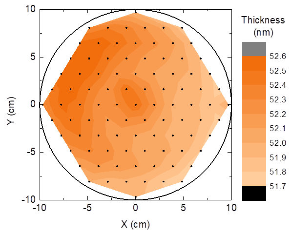
Within wafer thickness uniformity |
<±1.0% |
Wafer-to-wafer thickness repeatability |
<±1.0% |
Breakdown voltage |
≥7.0 MV/cm |
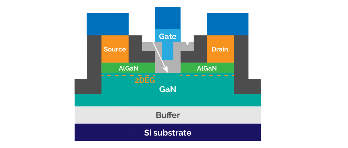
New GaN power electronics are being developed for power conversion and delivery. The high mobility and breakdown voltage of GaN make it an ideal material for power devices. There are several strategies to create such devices and using recess etching of the AlGaN barrier is a prominent one. Furthermore, gate dielectric layers are desired to limit leakage currents.
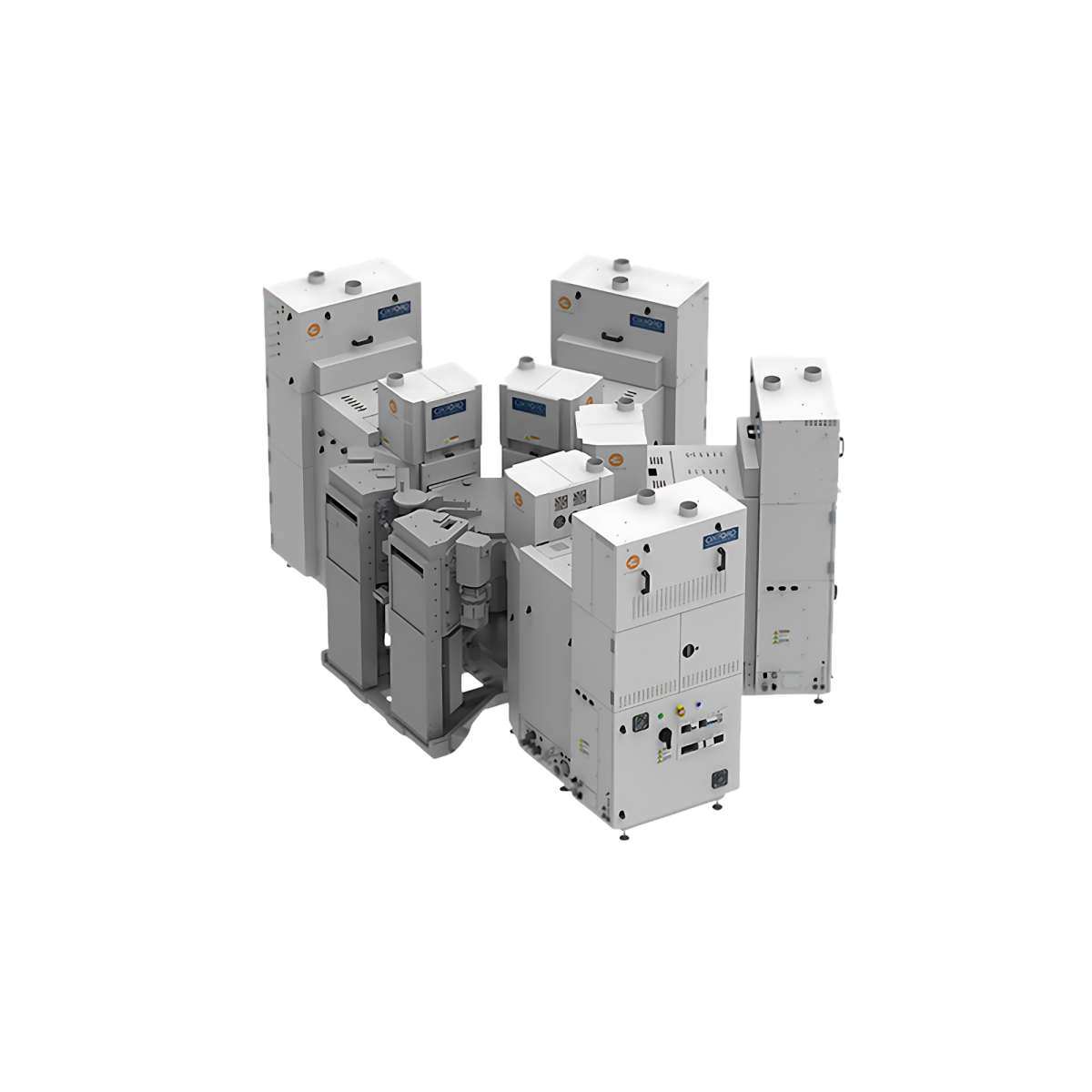
Watch this webinar from July 2019 anytime on-demand. Our ALD expert, Dr Aileen O'Mahony gives a masterclass in ALD for GaN. We look at how you can achieve excellent uniformity, optimised process conditions for low substrate damage, high material quality for superior device performance and conformal deposition. The webinar also includes an introduction to the Atomfab ALD system.