Part of the Oxford Instruments Group
Expand
Collapse
Part of the Oxford Instruments Group
Atomic Scale Processing means wafer-scale processing with control at the atomic scale. This atomic-level control extends to deposition of thin films, removal or etching of material, and growth of 1D and 2D materials with their distinctive unique properties such as graphene.
Our range of plasma processing systems provides a complete solution to Atomic Scale Processing. We provide unique cluster capability or stand alone systems enabling the manipulation of matter with atomic scale precision on a production scale.
Atomic Layer Etch (ALE) of Silicon, GaN & 2D materials
Atomic layer deposition of dielectrics, nitrides and metals with low damage. Our unique cluster capability provides the ability to cover surfaces directly without exposure to air. For instance these could be etched interfaces or freshly grown 2D materials such as MoS2 or graphene covered by ALD dielectrics or capping layers which can be a big advantage for a wide range of devices.
Atomic layer deposition of dielectrics & metals with low damage
The video above shows the ALD process in the FlexAL chamber.
Chemical Vapour Deposition & ALD of atomically thin structures: 1D & 2D materials.
Unique devices can be constructed by covering nanowires with ALD films or etching 1D and 2D materials to tune their properties.
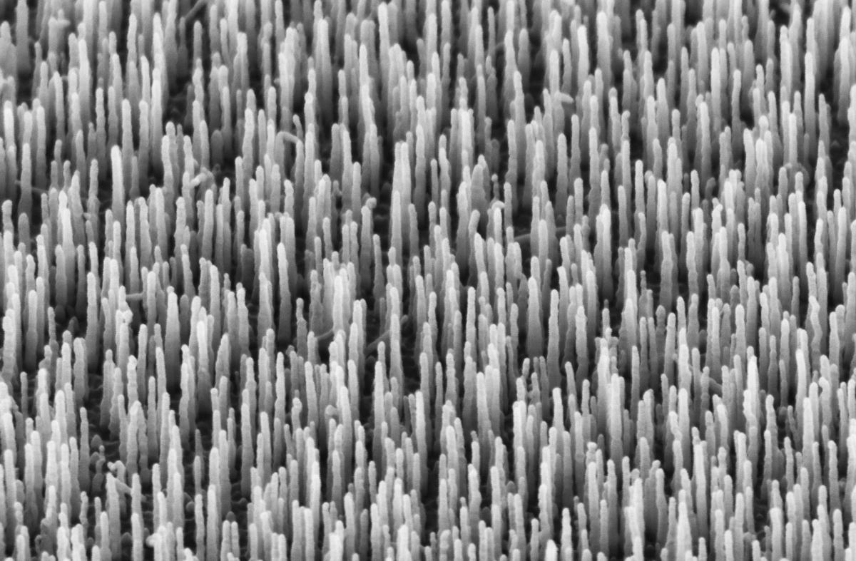
CVD growth of ZnO nanowires using DEZn precursors.
(Courtesy of Nanoscience Centre, Univ. of Cambridge)
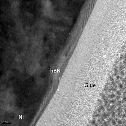
CVD growth of hBN
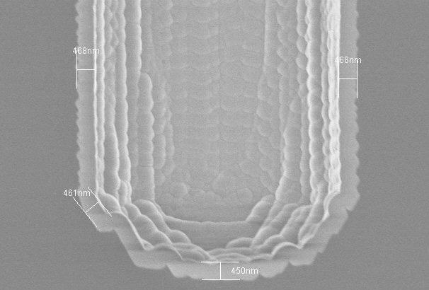
Atomic layer etching of Silicon, GaN & 2D materials. As these materials perform essential functions in a wide range of devices, our ability to etch these with extreme control and low damage can be an enabling technology. Furthermore combining ALE with deposition and growth will provide unique advantages in your device making.
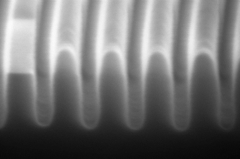
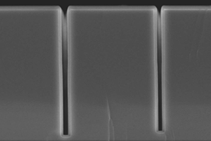
25nm wide Si trenches etched to 110nm depth by ALE, HSQ mask still in place.
PlasmaPro ASP delivers a step-change in capability with rapid, high-rate deposition of conformal, tunable oxides and nitrides.
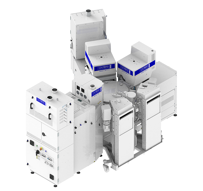
PlasmaPro ASP easily configures with other systems for advanced R&D

© Oxford Instruments 2025