 Part of the Oxford Instruments Group
Expand
Collapse
Part of the Oxford Instruments Group

With quantum technologies making the transition from laboratory demonstrations to scalable, manufacturable systems, the demands placed on materials and processes are intensifying. Achieving reliable qubit performance, ultra-low loss photonics, and repeatable device architectures all hinge on atomic-scale control of thin films, interfaces, and surfaces. Alongside more conventional and longstanding fabrication techniques, atomic layer deposition (ALD) and atomic layer etching (ALE) are becoming trusted processes for advancing quantum technologies.
As the name suggests, ALD and ALE are essential for achieving atomic-scale process control. Both technologies play vital roles in engineering precise and uniform materials, often enabling material thickness control at the Ångstrom scale. ALD enables the growth of complex, ultra-thin films with exceptional thickness and stoichiometric control, while ALE allows the layer-by-layer removal of material, ensuring dimension and surface damage control. At Oxford Instruments these technologies are seamlessly integrated into our quantum solutions. Across superconducting, photonic, and colour centre quantum modalities, our systems address the needs of both quantum information processing and quantum sensing devices.
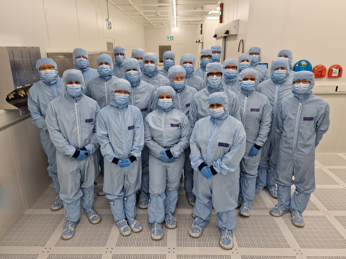
Figure 1: Oxford Instruments Plasma Technology's cleanroom team in state-of-the-art facility, Bristol, UK.
Our plasma enhanced ALD (PEALD) development platform, PlasmaPro ASP, and production PEALD platform, Atomfab, share design DNA, allowing processes developed in research environments to be transferred rapidly and reliably into manufacturing. PEALD combines the self-limiting nature of ALD with the additional tuneability and flexibility provided by a remote plasma source. PEALD has been demonstrated to enable lower impurity content, shorter cycle times, and enhanced tunability compared to thermal ALD. Both our PEALD systems share the same patented plasma source architecture and user interface, reducing risk during scale up. (To learn more about these complementary systems, check out the article from Semi Interface issue 3). For quantum technologies, device architectures and the materials in them are evolving rapidly, and it is therefore necessary to iterate multiple versions of devices with different film properties to stay ahead of the game. However, while chasing improved performance one eye must be kept on the eventual scalability of device and process solutions. Continuity between our two systems provides a practical pathway from early-stage innovation to manufacturable solutions.
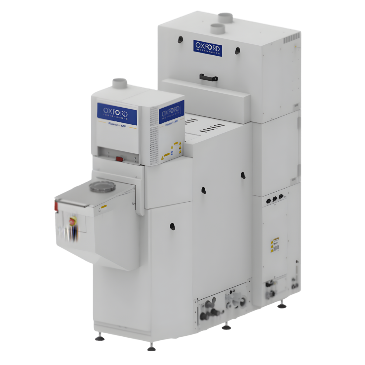
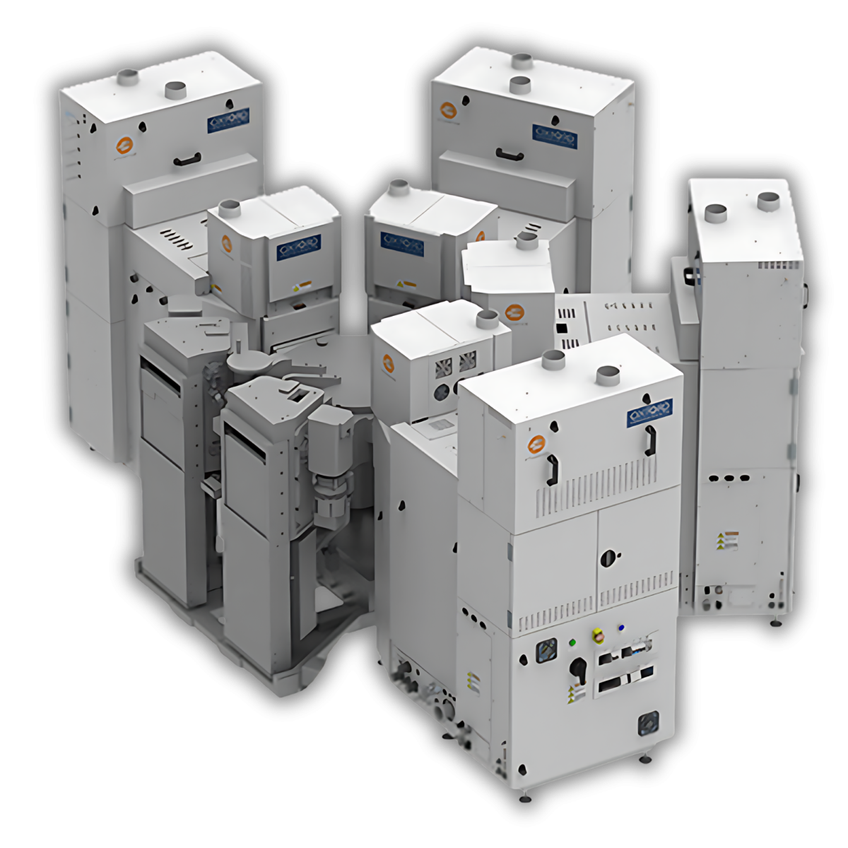
Figure 2 & 3: (Left) PlasmaPro ASP our PEALD development platform designed for rapid process development. (Right) Atomfab (four in a cluster), built with the same plasma source as the ASP and targeting PEALD for production environments.
For ALE, our PlasmaPro 100 Cobra ALE system offers Ångstrom-level etch control, providing smooth surfaces, high selectivity, and minimal plasma damage to surfaces and interfaces. One of the leading causes of loss across different modalities of quantum sensing and computing is etch induced damage, and ALE provides a route towards minimising this. Outside the quantum space, ALE is already being applied to enable low damage fabrication. For example, in complementary metal-oxide-semiconductor (CMOS), microLED and metal-insulator-semiconductor high-electron mobility transistor (MISHEMT) device fabrication, low damage ALE processes have been demonstrated to improve device performance. For quantum, ALE is largely untested territory, however literature reports indicate that it may provide similar benefits. The Cobra ALE system is compatible with wafers of up to 200 mm and can be equipped with a single wafer loadlock, cassette handler, or as part of a cluster.
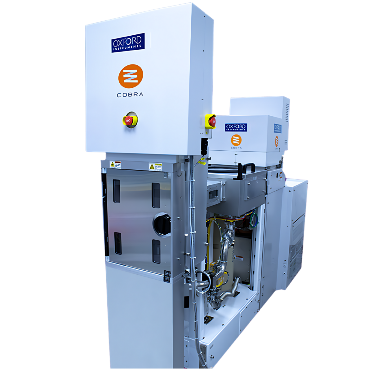
Figure 4: Cobra ALE system attached to an automated cassette handler to enable high throughput processing for both ALE and ICP-RIE.
This summer, the AVS 26th International Conference on ALD, combined with the 13th International ALE Workshop, will be held in Florida, USA. Tampa will become the hub for ALD and ALE experts from around the world, bringing together researchers, engineers, and industry leaders to share the latest advances in these precision process technologies, where quantum is increasingly becoming part of the conversation. In fact, quantum has its own session - Quantum ALD Applications - moderated by our own Dr Arpita Saha.
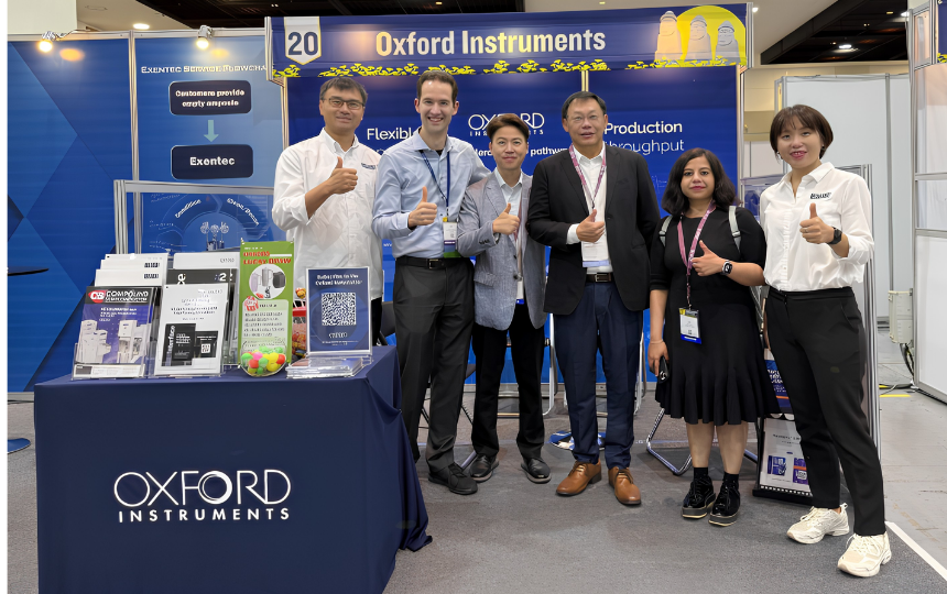
Figure 5: Oxford Instruments Plasma Technology's team at the AVS International Conference, 2025.
Oxford Instruments will be there to exhibit our advanced ALD and ALE solutions, highlighting how the team of in-house engineers and researchers-in-residence are developing these technologies to address the challenges of scaling and performance for next-generation devices. Dr. Arpita Saha, Deposition Solutions Manager, and Dr. Harm Knoops, Atomic Scale Segment Specialist, both sit on the ALD and ALE Steering Committees, respectively. In addition to moderating sessions, alongside other Oxford Instruments colleagues, they will present innovative research for advanced quantum and power electronics devices. Here is a quick look at this year’s topics…
Superconducting Nitrides by Fast Remote Plasma ALD for Quantum Applications
Dr Harm Knoops - Atomic Scale Segment Specialist
High Rate, Tuneable Dielectric Nitrides by Plasma Atomic Layer Deposition Enabling Volume Manufacturing for GaN Device Integration
Dr Arpita Saha - Deposition Solutions Manager
Examining AlGaN Atomic Layer Etch per Cycle Uniformity and Repeatability by Cross-Referencing In-Situ Etch Depth Monitoring with Electrical Characterisation
Dr Ben Jones - Applications Engineer
Multi-Cycle Plasma Enhanced Atomic Layer Deposition of Superconducting Nitride Structures for Photonics and Quantum Computing Applications
Dr Nick Chittock - Quantum Technologies Market Specialist
Collaborator contributions
Talk; Precise and narrow ion-energy distributions in plasma-enhanced ALD of nitrides using tailored-waveform biasing
Dr Adrie Mackus - Eindhoven University of Technology
Talk; Directional atomic layer etching of MgO-doped lithium niobate using Br-based plasma.
Poster; Improving optical resonator quality factors in thin-film lithium niobate with atomic layer etching
Ivy Chen - Caltech
Talk; Atomic layer etch process for Nb and Ta using CF4/H2 plasma
Ryan Walsh - University of Nevada, Reno
Poster; Numerical and experimental investigations on tailored waveforms
Dr Sebastian Mohr & Lucy Manukyan, Quantemol ltd.
We’ll be diving deeper into the technologies shaping the quantum future in our next edition, including more on how our atomic scale processing technologies are enabling next-generation quantum devices.
Explore previous editions here:
Explore Semi Interface MagazinePeeters, S. A.; Nelissen, L. E. W. H. M.; Besprozvannyy, D.; Choudhary, N.; Lennon, C. T.; Verheijen, M. A.; Powell, M.; Bailey, L.; Hadfield, R. H.; (Erwin) Kessels, W. M. M.; Knoops, H. C. M. Superconducting Nb x Ti1− x N Prepared at High Deposition Rates with Plasma-Enhanced Atomic Layer Deposition and Substrate Biasing. AVS Quantum Science 2025, 7 (2). https://doi.org/10.1116/5.0254....
Shiravand, I.; Jamalzadeh, M.; Nguyen, M.; Nadeau, C.; Perez, M. M.; Hwang, S.; Tong, X.; Nykypanchuk, D.; LaHaye, M.; Shahrjerdi, D. Investigation of Kinetic Inductance and Microwave Loss in Thin-Film TaCxN1−x Superconducting Resonators. Appl Phys Lett 2025, 127 (19). https://doi.org/10.1063/5.0300....
de Leon, N. P.; Itoh, K. M.; Kim, D.; Mehta, K. K.; Northup, T. E.; Paik, H.; Palmer, B. S.; Samarth, N.; Sangtawesin, S.; Steuerman, D. W. Materials Challenges and Opportunities for Quantum Computing Hardware. Science (1979) 2021, 372 (6539). https://doi.org/10.1126/scienc....
Honda, M.; Katsunuma, T.; Tabata, M.; Tsuji, A.; Oishi, T.; Hisamatsu, T.; Ogawa, S.; Kihara, Y. Benefits of Atomic-Level Processing by Quasi-ALE and ALD Technique. J Phys D Appl Phys 2017, 50 (23), 234002. https://doi.org/10.1088/1361-6....
Liu, T.; Liu, Z.; Cao, H.; Nong, M.; Tang, X.; Jiang, Z.; Garcia, G. I. M.; Ren, K.; Li, X. Significant Improvement of Breakdown Voltage of Al0.86Ga0.14N Schottky Barrier Diodes by Atomic Layer Etching. Appl Phys Lett 2025, 126 (15). https://doi.org/10.1063/5.0251....
Liu, Z.; Cao, H.; Liu, T.; Lu, Y.; Tang, X.; Jiang, Z.; Xiao, N.; Li, X. Alleviate Sidewall Damage of InGaN Green Micro-LEDs by Atomic Layer Etching. Opt Lett 2025, 50 (11), 3756. https://doi.org/10.1364/OL.561....
Michaels, J. A.; Delegan, N.; Tsaturyan, Y.; Renzas, J. R.; Awschalom, D. D.; Eden, J. G.; Heremans, F. J. Bias-Pulsed Atomic Layer Etching of 4H-Silicon Carbide Producing Subangstrom Surface Roughness. Journal of Vacuum Science & Technology A 2023, 41 (3). https://doi.org/10.1116/6.0002....
Hossain, A. A.; Murphy, S.; Catherall, D. S.; Ardizzi, A. J.; Minnich, A. J. Atomic Layer Etching of Niobium Nitride Using Sequential Exposures of O2 and H2/SF6 Plasmas. Journal of Vacuum Science & Technology A 2025, 43 (4). https://doi.org/10.1116/6.0004....
Quantum Technologies Market Specialist at Oxford Instruments Plasma Technology
Prior to joining Oxford Instruments, Nick gained his PhD working in Professor Erwin Kessels’ group at Eindhoven University of Technology, specialising in Atomic Layer Etch and working in collaboration with Oxford Instruments on the development of processes for ALE and ALD. Nick manages the ALE page of the Atomic Limits website in collaboration with TU/e. In his current role he aims to improve the fabrication of quantum devices by leveraging advanced nanofabrication techniques, such as ALD and ALE.
Semiconductor Marketing and Technology Specialist, Oxford Instruments Plasma Technology
She studied chemistry at University College Cork (UCC). After graduating in 2017, Emma undertook her PhD at Tyndall National Institute/ UCC, researching 2D transition metal dichalcogenides as next-generation semiconductor materials, under the supervision of Professor Paul Hurley


© Oxford Instruments 2026

