Part of the Oxford Instruments Group
Expand

Atomic Layer Etching (ALE)

Atomic Layer Etching (or ALE) is an advanced etch technique that allows for excellent depth control on shallow features. As device feature size reduces further and further ALE is required to achieve the accuracy required for peak performance.

High fidelity pattern transfer (etching) is essential for the fabrication of today’s advanced microelectronic devices. As features shrink to sub-10nm levels, and novel devices make use of ultra-thin 2D materials, there is an increasing need for atomic-scale fidelity.

This has led to a growing interest in a technique known as Atomic Layer Etching (ALE), which overcomes the limitations of conventional (continuous) etching at the atomic scale. Plasma-based atomic layer etching is a cyclical etching process of gas dosing and ion bombardment that removes material layer by layer and has the potential to remove single atomic layers with very low damage.


Process Benefits

  • Achieves etching of layers with high depth accuracy
  • Up to 200 mm wafer with typical uniformity <±2%
  • Advanced technology for high control of etch depth
  • Low damage to underlying substrates
  • Can be used in combination with standard ICP
Request more information Download brochure

Atomic layer etching process

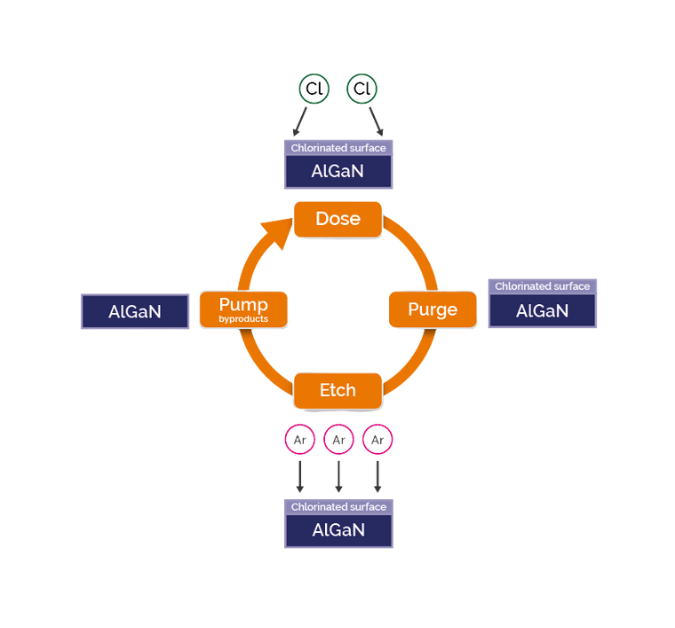
Atomic Layer Etching typically involves a cycle of 4 steps that is repeated as many times as necessary to achieve the required etch depth. This example shows ALE of AlGaN etching with Cl2/Ar.

Step 1) Dosing of the substrate with an etching gas, which adsorbs on and reacts with the etch material. The etch gas is often plasma dissociated to enhance the rate of adsorption. With the correct choice of dosing gas and parameters, this can be self-limiting, if the chemical dose stops after adsorbing one monolayer.

Step 2) Purging of all residual dose gas.

Step 3) Bombardment of the surface with low energy inert ions which removes the reacted surface layer. This can be self-limiting if the energy of the ions is sufficient to remove the chemically modified layer, but insufficient to (sputter) etch the underlying bulk material.

Step 4) Etching products are purged from the chamber.

ALE Process of Si With Cl2 Ar

Benefits of Atomic Layer Etching

  • Low damage etching, due to the use of low ion energies
  • Precise control of etching depth
  • Ultra-thin layer removal
  • Self-limiting behaviour
  • High selectivity, since dose gas and ion energy can be tailored to minimise etching of mask layers or underlying materials
  • Etch rate is less affected by the aspect ratio of etched features (i.e. reduced ARDE), since the supply of radicals and surface ion bombardment have been separated into independent steps
  • Improved uniformity, due to its self-limiting nature
  • Smooth etch surfaces
  • Anisotropic in nature, due to the reliance on ion bombardment
Read the article

Atomic Layer Etching: What for?

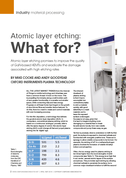
Read our article in Compound Semiconductor

Atomic layer etching promises to improve the quality of GaN-based HEMTs and eradicate the damage associated with high etching rates.

Written by Dr Mike Cooke and Dr Andy Goodyear for Compound Semiconductor magazine.

ALE Features

  • Etch rates 2 to 7Å/cycle
  • Demonstrated results in a-Si, Si, SiO2, MoS2, GaN, AlGaN layer etching
  • Fast recipe control down to 10ms
  • Atomic Layer Deposition-style gas dose delivery with 10ms open-close response
25nm wide Si trenches etched to 110nm depth by ALE, HSQ mask still in place

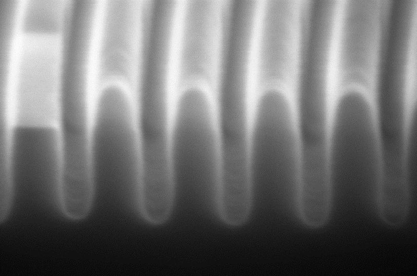
25nm wide Si trenches etched to 110nm depth by ALE, HSQ mask still in place.

ALE of MoS2 shows no Raman defect

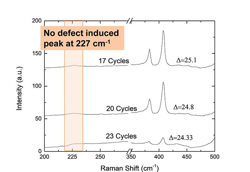
ALE of MoS2 shows no Raman defect peak after etching, highlighting the low damage etching capabilities of ALE.

AlGaN surface roughness after 200 ALE cycles

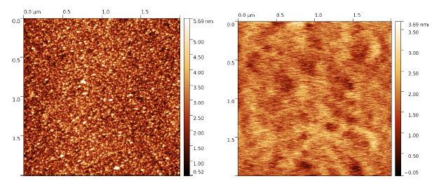
AlGaN surface roughness after 200 ALE cycles, left = before etching (Ra = 600pm), right = after etching (Ra = 300pm). The surface has been smoothed by ALE.

Wide range of materials

ALE is suitable for a wide range of materials, including Si, a-Si, MoS2, SiO2, GaN, AlGaN, III-V’s, Si3N4, graphene, HfO2, ZrO2, Al2O3, metals etc.

    Material etched

    Dose gas

    Etch gas

    MoS2

    Cl2

    Ar

    Si or a-Si

    Cl2

    Ar

    SiO2

    CHF3 or C4F8

    Ar or O2

    AlGaN or GaN

    Cl2, BCl3

    Ar

    AlGaN or GaN

    N2O

    BCl3

    GaAs or AlGaAs

    Cl2, BCl3

    Ar

    InP or InGaAsP etc.

    CH4, Cl2

    Ar

    SiN

    H2

    Ar

    Al2O3

    BCl3

    Ar

    Graphene

    O2

    Ar

    HfO2, ZrO2

    Cl2, BCl3

    Ar

    ALE AlGaN cycle

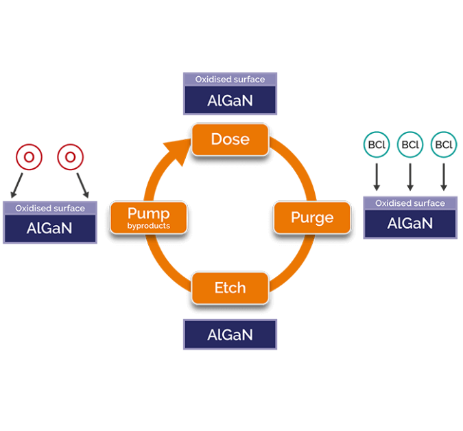
    AlGaN ALE Process Cycle

    AlGaN EPC

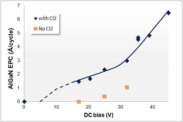
    AlGaN Etch per Cycle with and without Chlorine dose

    Featured ALE Products

    PlasmaPro 100 ALE

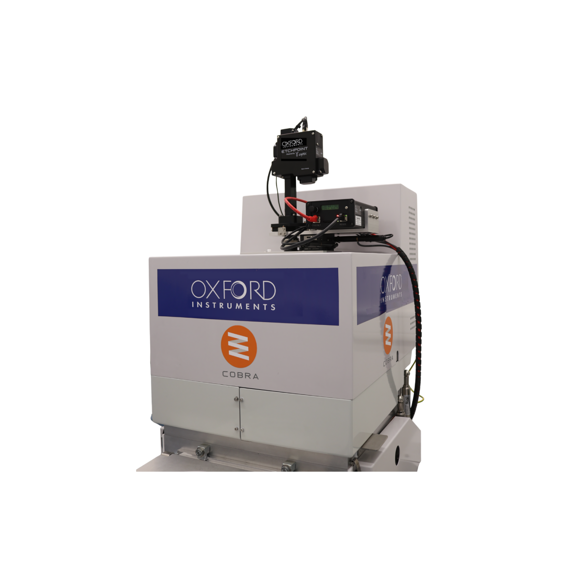
    The PlasmaPro 100 ALE delivers precise process control of etching for next-generation semiconductor devices. Specially designed for processes such as recess etching for GaN HEMT applications and nanoscale layer etching, the system's digital/cyclical etch process offers low damage, smooth surfaces.

    • Digital/Cyclical etch process – etching equivalent of ALD
    • Low damage
    • Smooth etch surface
    • Superb etch depth control
    • Ideal for nanoscale layer etching (e.g. 2D Materials)
    • Wide range of processes and applications
    Request more information

    As layers become thinner to enable the next-generation semiconductor devices, there is a need for ever more precise process control to create and manipulate these layers. The PlasmaPro 100 ALE delivers this by enhancing our Cobra ICP platform with specialised hardware for atomic layer etching.

    • Delivers reactive species to the substrate, with a uniform high conductance path through the chamber - Allows a high gas flow to be used while maintaining low pressure
    • Variable height electrode - Utilises the 3-dimensional characteristics of the plasma and accommodate substrates up to 10mm thick at optimum height
    • Wide temperature range electrode (-150°C to +400°C) which can be cooled by liquid nitrogen, a fluid re-circulating chiller or resistively heated - An optional blow out and fluid exchange unit can automate the process of switching modes
    • A fluid controlled electrode fed by a re-circulating chiller unit - Excellent substrate temperature control
    • RF powered showerhead with optimised gas delivery - Provides uniform plasma processing with LF/RF switching allowing precise control of film stress
    • ICP source sizes of 65 mm, 180 mm, 300 mm - Delivers process uniformity up to 200 mm wafers
    • High pumping capacity - Gives wide process pressure window
    • Wafer clamping with He backside cooling - Optimum wafer temperature control
    Request more information
    • Low damage p-GaN HEMTs and recessed gate MISHEMTs etch for power electronics and RF devices
    • 2D materials patterning/thinning
    • Nanostructured SiO2, Si, SiN
    • III-V materials
    • Solid-state lasers InP etch
    • VCSEL GaAs/AlGaAs etch
    • Hard mask deposition and etch for high brightness LED production
    • SiO2 and quartz etch
    Download brochure
    Request more information

    PlasmaPro 100 Atomic Layer Etch with Etchpoint

    For GaN Power Electronics & RF Applications

    Oxford Instruments’ PlasmaPro 100 Atomic Layer Etch (ALE) solution delivers precise etching control for cutting-edge specifications and performance requirements of GaN HEMTs manufacturers. With a fully-integrated Etchpoint® etch depth monitoring solution optimised for GaN and AlGaN layers, the PlasmaPro 100 ALE system combined provides low damage etching with surface smoothing with unparalleled accuracy in target etch depth for devices such as p-GaN HEMTs and recessed gate MISHEMTs.
    The fabrication of GaN HEMTs for power electronics and RF applications is experiencing a massive production ramp driven by the need for efficient, high-performance devices for integration in a wide range of products such as mobile device chargers, electric vehicles, base station transceivers, and data centres.
    Download brochure
    Request more information

    Key Benefits of PlasmaPro 100 ALE and Etchpoint solution

    • High rate ICP and low damage ALE processing of GaN and AlGaN in the same chamber up to 200 mm
    • Excellent process etch uniformity for improved device and wafer yield
    • Production-proven etching platform trusted for high-volume manufacturing with automated cassette handler
    • Patent-pending UV wavelength Etchpoint etch depth monitor developed with LayTec and optimised specifically for GaN and AlGaN etching
    • Exceptional post-etch remaining AlGaN thickness accuracy of ±0.5 nm enabled by Etchpoint endpoint detection
    • Reduced AlGaN and GaN surface roughness with ALE processing for improved GaN HEMT performance

    GaN Power Electronics & RF Applications

    5G base stations

    5G-based stations

    Efficient power suppliers for data centres

    Efficient power suppliers for data centres

    Fast chargers for EV

    Fast chargers for EV

    Fast mobile devices charging

    Fast mobile devices charging


    Performance benefits for GaN HEMTs using ALE and Etchpoint

    ALE and Etchpoint for p-GaN HEMTs

    • Accurate control of p-GaN etch depth with Etchpoint EPD
    • Low damage “soft-landing” onto AlGaN surface by ALE after high rate ICP etch of GaN
    • Low roughness, surface smoothing to enable better performance normally-off HEMT devices

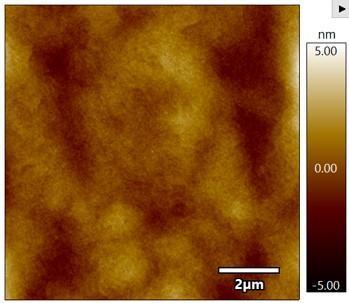
    Figure caption (LHS): Higher AlGaN surface roughness (0.8 nm Ra) for ICP-RIE process.

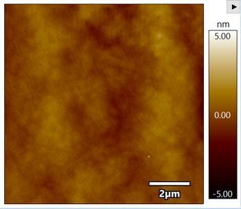
    Figure caption (RHS): Reduced AlGaN surface roughness (0.4 nm Ra) for ICP-RIE & ALE process.

    pganhemt

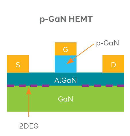
    Figure caption: ALE for surface smoothing, low roughness processing of p-GaN devices to enable improved device performance.


    ALE & Etchpoint solution for recessed gate MISHEMT

    • Low etch rate, low damage, controlled ALE process for <25 nm AlGaN layer etching with typically 0-5 nm AlGaN remaining in recessed gate region
    • Etch thickness accuracy of ±0.5 nm for remaining AlGaN layer to enable normally-off device behaviour and improved device reliability
    • Normally-off recessed gate MISHEMT demonstrated
    • Low surface roughness with surface smoothing of the remaining AlGaN (partial etched recess) or GaN (fully etched recess) surface

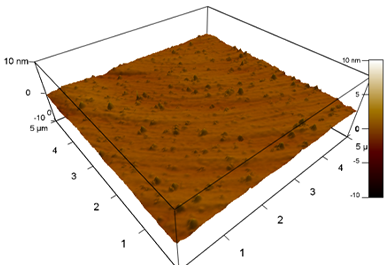
    Figure caption (LHS): GaN surface roughness (0.2 nm Ra) before ALE to demonstrate fully-recessed device with through-AlGaN etch.

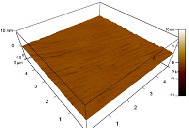
    Figure caption (RHS): GaN surface roughness (0.1 nm Ra) after ALE to demonstrate fully-recessed device with through-AlGaN etch.

    mishemt

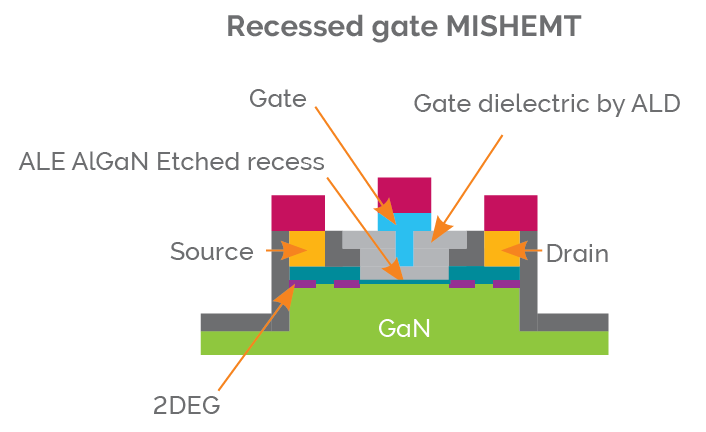
    Figure caption: ALE for accurate etch thickness control of remaining AlGaN to ±0.5 nm for partially-etch recess to enable normally-off devices and improved device reliability.

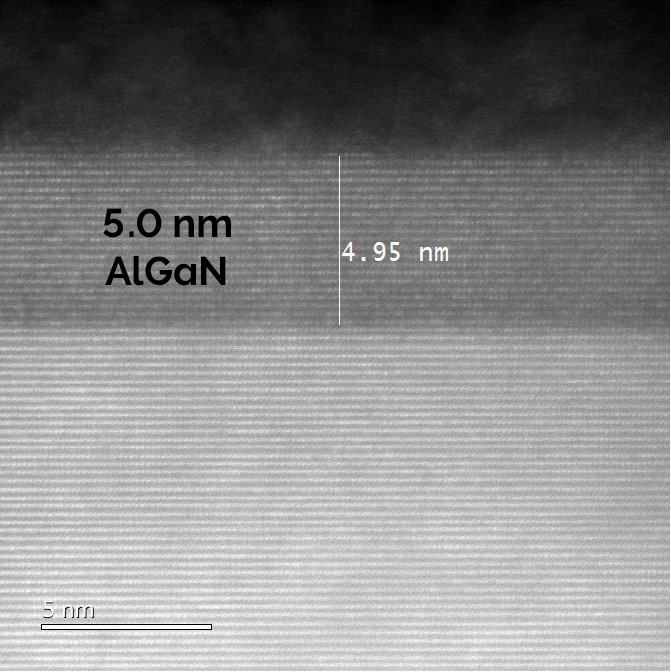
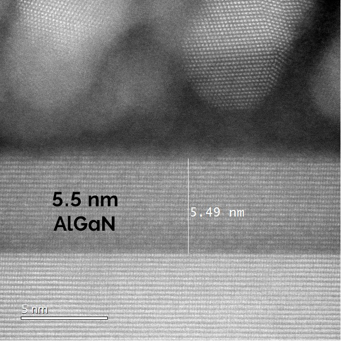
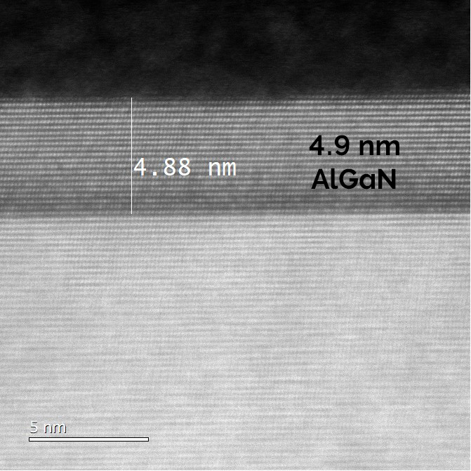
    Figure caption: TEM verification across 3 samples of Etchpoint accuracy for AlGaN layer. Targeted AlGaN remaining thickness after ALE of 5 nm ±0.5 nm achieved, which was correlated to Etchpoint etch traces.


    Etchpoint Etch Depth Monitor

    Etchpoint is a patent-pending UV reflectance-based endpoint technique with the optimised wavelength selected to allow for unrivalled accuracy of etch layer depth for GaN and AlGaN. Other endpoint solutions can typically achieve ±2 nm resolution which limits the capability to reliably fabricate some GaN HEMT device structures. This new etch-depth monitoring solution has been exclusively developed and optimised by Oxford Instruments in collaboration with LayTec. Etchpoint is fully integrated with both the hardware and software of the PlasmaPro 100 ALE system.

    Etchpoint product features

    • UV reflectance-based endpoint
    • Spot size of ~300 µm
    • Measurement of the EPD stop signal measurement based on reflection of UV light on an unstructured test pad of 500 x 500 µm
    • Automatically reaches the measurement position with a 5 x 5 mm area search before the etch process commences
    • Fully integrated software interface between Etchpoint and the system PTIQ control software
    • Configured with tiltable measurement head and motorized XY-stage for the test pad search
    • Exceptional post-etch remaining AlGaN thickness accuracy of ±0.5 nm enabled by Etchpoint endpoint detection
    etchpoint

    Highly-configurable, flexible systems

    Cluster Options

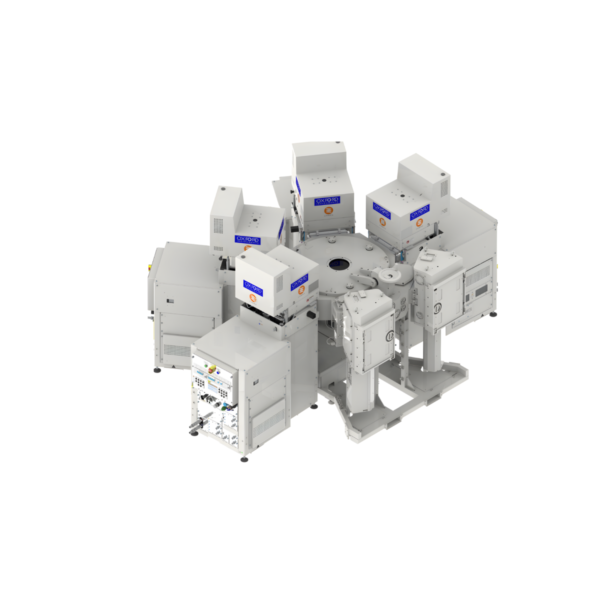
    Platforms may be clustered to combine technologies and processes with either cassette or single wafer loading options. Hexagonal or square transfer chamber configurations are available.

    Cobra Single-Cassette Cluster
    Cobra Single-Cassette Cluster
    Cobra Twined-Cassette Cluster
    Cobra Twined-Cassette Cluster