 Part of the Oxford Instruments Group
Expand
Collapse
Grab a first-class seat at a world-class venue with the some of the best compound semiconductor experts at Oxford In Your City, an exclusive seminar event for device manufacturers.
Hear the latest insights on low damage plasma etch & deposition solutions for device manufacturing, with topics including VCSELs, GaN, ALE, ALD and InP.
Held at the famous RMS Queen Mary, the venue offers stunning views of the Long Beach coastline. After lunch, you'll also have a guided tour of the ship.
Don't miss out! Places are limited so save your seat today.
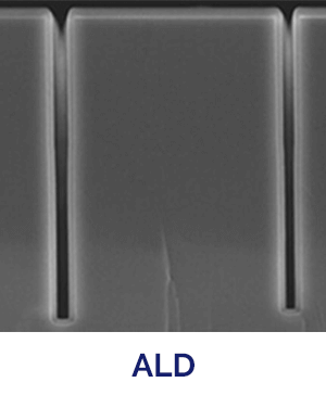
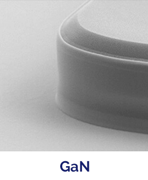
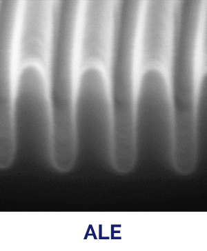
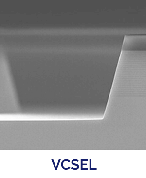
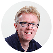
Dr Mark Dineen has over 20 Years of plasma processing experience. His more recent work includes applying this knowledge to a wide range of devices from semiconductor lasers to GaN based RF devices.
Dr Dineen is now an Experienced Technical Marketing Manager with a demonstrated history of communicating complex technical ideas and scientific concepts to a varied audience. These technologies include ALD, ALE, CVD, ICP, PECVD and RIE plasma processing and cover how these can deliver device solutions to our customers.

Stephanie obtained her degree from the University of Orleans, France, in Optics, Lasers & Plasma. Now, in her Senior Technical Marketings role, she closely follows and works with optoelectronics device manufacturers to translate next-generation device characteristics and requirements into plasma processing solutions and products. Stephanie has been intimately involved in understanding and developing our best-in-class VCSEL processing solutions.
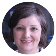
After receiving her PhD (funded by Intel and Science Foundation Ireland) from University College Cork, Ireland, her professional career has revolved around Atomic Layer Deposition (ALD) technology. Aileen brings broad international experience and has worked both in the US and UK. She joined Oxford Instruments 4 years ago and is currently our Atomic Scale Product Manager, focused on the market introduction of a new high-speed ALD system called Atomfab™, developed exclusively for the production market.
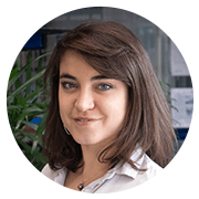
Pauline Alvarez received her masters degree in Physics from the Institut National des Sciences Appliquees de Toulouse, France, where she specialized in Micro-Nanophysics. She was first introduced to Ion Beam Sputtering while working at CEA Leti, Grenoble, France, where she deposited group II-VI passivation coatings for infrared applications using an Ionfab 300 to study the relation between synthesis, microstructure and thin film properties.

With over 15 years of atomic force microscopy (AFM) experience, Mayur is the Director of Sales for Asylum Research, focusing on AFM metrology for industrial and research applications. He has a bachelors in Electrical Engineering and a masters in Bio Engineering from Ohio State University.
We also have two other exclusive events being held in Santa Barbara, CA on March 25 and San Jose, CA on March 26.
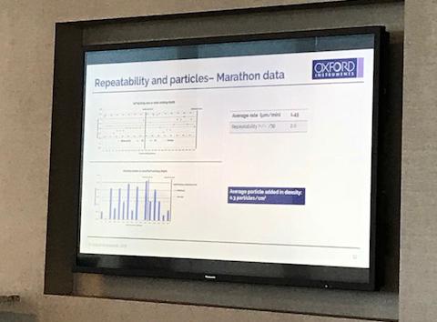
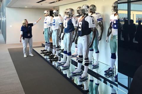
Our last event was held at the famous Dallas Cowboys World Headquarters in Frisco, Texas, which involved a fantastic day of talks on all things compound semiconductor. Guests also enjoyed a guided tour of the stadium, The Star.
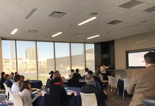
"Cutting edge tech will help us with our VCSEL fabrication."
"VP-level representation showed great commitment and support."
"It was well-organised and had very knowledgable presenters."
