Part of the Oxford Instruments Group
Expand
Collapse
Part of the Oxford Instruments Group
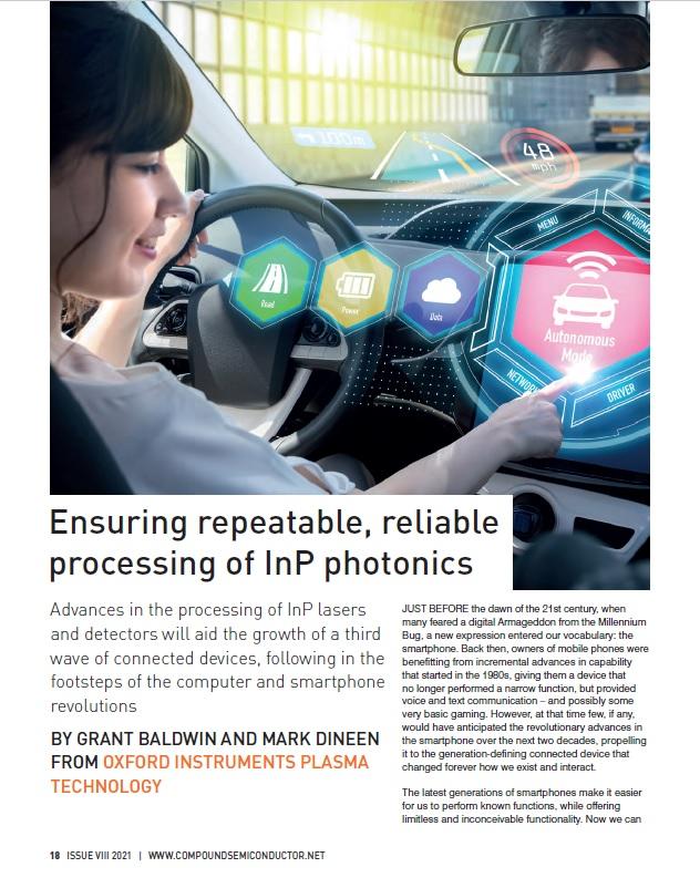
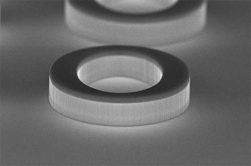
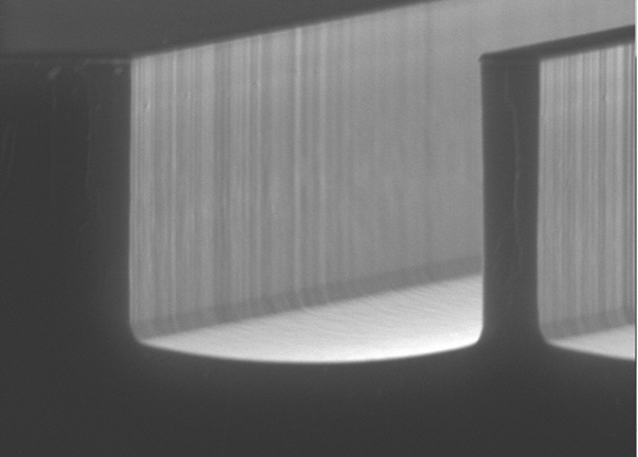
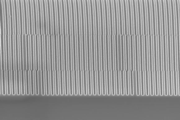
To ensure the desired electronic performance, InP devices are manufactured using complex multistep epitaxial deposition, masking and plasma-etch processes. We offer a market-leading range of InP process solutions, from slow etch for fine features, such as gratings, to solutions for etching ultra-smooth structures, enabling engineers to master the fabrication of InP devices.
We have III-V plasma technology solutions for volume manufacturing and niche development. To see what the next level of InP processing looks like, click to read our article.
Advances in the processing of InP lasers and detectors will aid the growth of a third wave of connected devices, following in the footsteps of the computer and smartphone revolutions.
Written by Grant Baldwin and Mark Dineen for Compound Semiconductor magazine.
InP enables the manufacture of components that can operate at high frequencies allowing higher volumes of data. Its superior electron mobility has established the (InP) a strong compound semiconductor material for the manufacturing of laser diodes, optoelectronics, high-frequency electronic, photonic integrated circuits and optical fibre for data communication.
When design and fabrication are optimised, InP lasers provide high spectral purity and optical power, over a wide temperature range. The achievable wavelength range of 1100 – 2000 nm is optimal for fibre optic communications. Our Plasma Technologies enable you to produce reliable InP devices, reducing optical losses and achieving the highest yield and throughput.

© Oxford Instruments 2026