Part of the Oxford Instruments Group
Expand
Collapse
Part of the Oxford Instruments Group
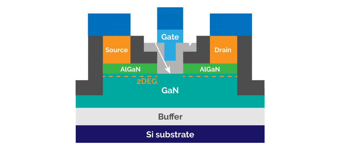
New GaN power electronic devices are being developed for power conversion and delivery, the high mobility and breakdown voltage of GaN making it an ideal material for power devices. In Electric and Hybrid Electric Vehicles (EV and HEV), these devices are becoming increasingly important and device cost and efficiencies are critical for their success. However, there are still manufacturing challenges that need to be addressed to achieve the device performance and full wafer yield needed.
‘E-mode’ devices are essential for the fail safe operation of power devices and several designs are used to achieve this ‘normally -off’ performance. Both p-GaN and recessed gate HEMT devices require innovative process solutions. Etch depth control, deposition of high-k dieletrics and low damage at ultra sensitive surfaces are all critical to device performance.
In this white paper, we discuss several strategies to create efficient GaN devices including the use of Atomic Layer Etching (ALE) for the recess etching of the AlGaN barrier and high throughput Atomic Layer Deposition (ALD) of Al2O3 for gate dielectric and passivation.
Download White Paper
Read more about how ALD can optimise GaN power devices in our white paper.
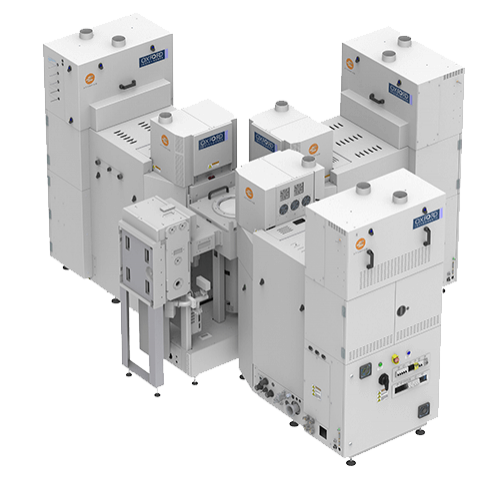
Download White PaperAtomfab is the fastest remote plasma production ALD system in the market. Its ALD technology offers precisely controlled ultra‑thin films for advanced applications on the nanometre scale, with conformal coating of sensitive substrates structures.

© Oxford Instruments 2026