 Part of the Oxford Instruments Group
Expand
Collapse
Part of the Oxford Instruments Group
by: Nazia Tabassum, Monash University, Australia
Microneedles have been demonstrated to facilitate enhanced transdermal delivery of active agents (e.g. macromolecules, nanoparticles, small polar molecules) otherwise impermeable to the skin. However, currently microneedles present number of disadvantages such as limited drug loading capacity and uncontrolled degradation. Recently, the microneedle scale is sizing down to the nano-scale, which could lead to remarkable advantages. Nanoneedles, i.e. micron-sized needles integrating nanoscale features, are particularly promising because of their increased surface area, reduced invasiveness, and pain-free administration. However, precise control of the over degradation rate of micro/ nanoneedles within the skin remains a great challenge. In our lab, we have developed porous silicon nanoneedles (pSiNNs) with tunable porosity, biodegradability and mechanical strength for non-invasive drug delivery that will improve the treatment of various diseases.
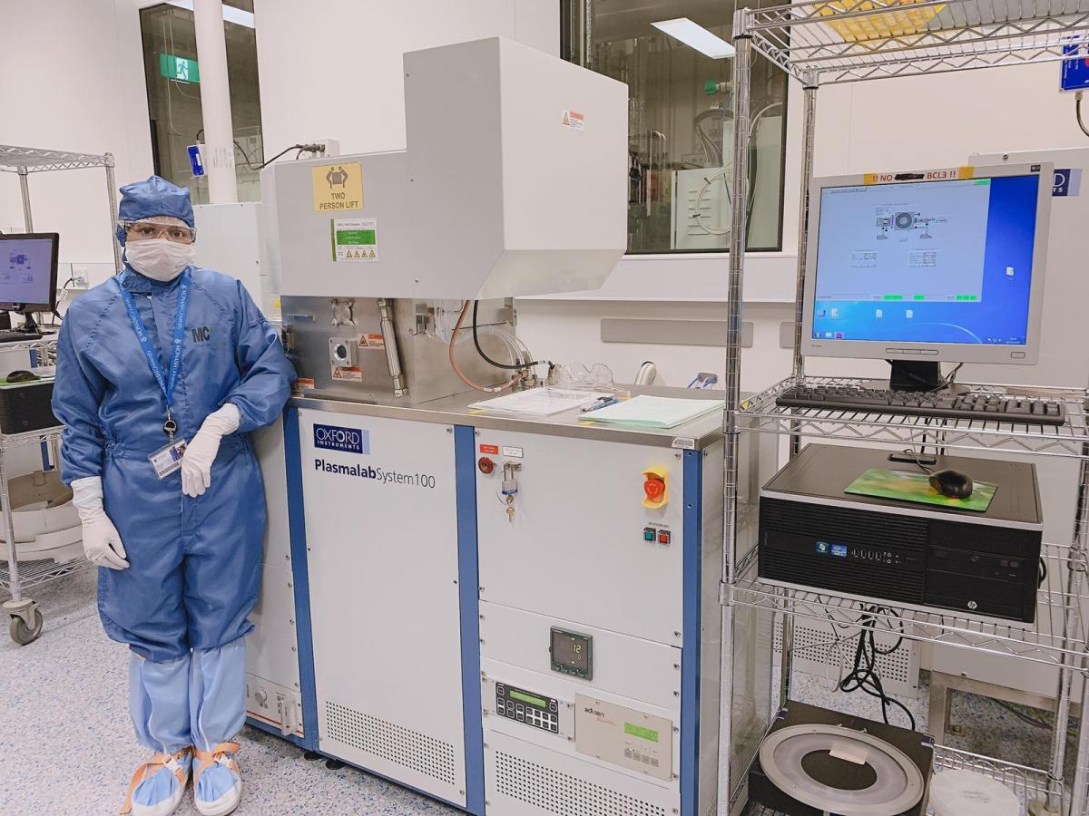
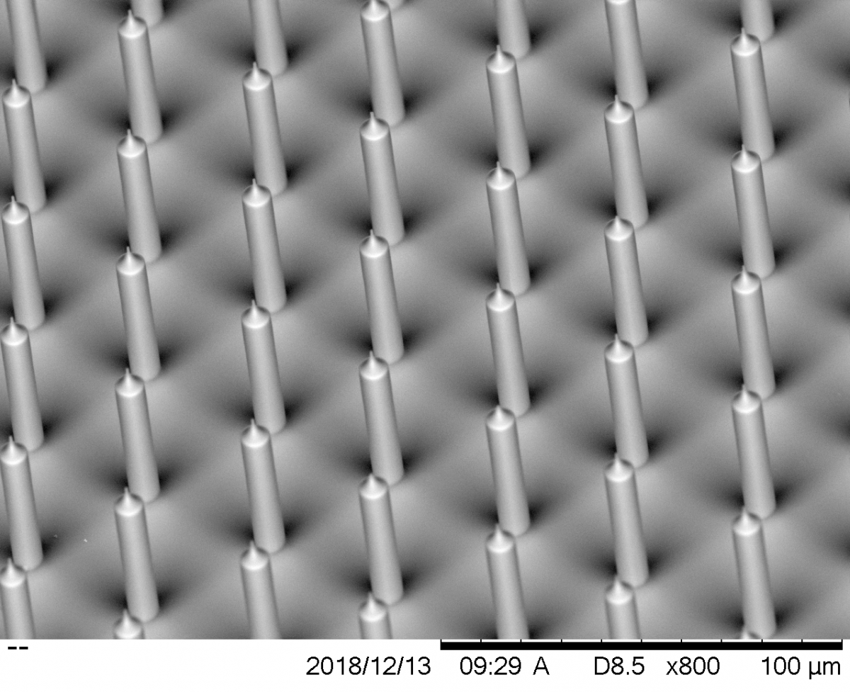
Nanoneedle arrays with a length of 40-50 μm and a tip diameter below 1 μm are fabricated using Oxford Plasma 100 deep reactive ion etching (DRIE) instrument. The Oxford Instruments’ Plasma DRIE allows us to create sharpened nanoneedle projections that are able to puncture the outermost layers of the skin and facilitate the delivery of therapeutic agents. The fabrication process consists of a UV photolithography patterning step followed by dry etching with the DRIE tool. Following, the nanoneedles are posified in a wet etching process by electrochemical anodisation. Further fabrication details are elaborated in the following paragraphs.
P-type, low resistivity silicon wafers are used as a starting substrate for the nanofabrication of vertical arrays. For this purpose, a silicon wafer is coated with positive photoresist (AZ®4562) by spin coating. The substrate is further baked at 110 ºC. A chromium mask is used to transfer the defined pattern on the substrate by UV exposure. The photosensitive-coated substrate is lastly immersed in AZ®400K developer solution where the exposed resist is removed to complete the photolithographic patterning of nanoneedles.
Si wafers containing photoresist-patterned circles are etched using an Oxford Plasmalab 100 DRIE by performing a Bosch process and by standard dry etching base on RIE. The fabrication of nanoneedle arrays is a three-step process consisting of isotropic sulphur hexafluoride (SF6) step to create a sharp tip, and Bosch process step to obtain cylindrical posts in an anisotropic etching. As a third step, the reshaping of nanoneedles is done with a mixture of SF6 and octafluorocyclobutane (C4F8) gases to obtain sharper tips for enhanced skin penetration.
1. SF6 only:
Firstly, the sharp tip of nanoneedle arrays is created by using isotropic SF6 etching process with controlled time. In isotropic SF6 etching, the flow rate of SF6 gas is adjusted. The ICP generator power and RF power are maintained.
2. Bosch process:
Bosch etching employs SF6 and C4F8 gases for the etching and passivation cycles, respectively. In both the cycles, the flow rate of C4F8 and SF6 is adjusted. Helium gas pressure is parametrised using the APC valve position and table temperature values. The desired depth of Si etching is proportionally achieved through etching and passivation cycles. The photoresist on the tip of nanoneedles array is later removed with acetone, isopropyl alcohol and water in a sonication bath of around one minute per solvent.
3. Porosification by electrochemical etching of silicon nanoneedles
Silicon wafers containing nanoneedle arrays are electrochemically etched in a hydrofluoric acid (48%) and ethanol (3:1 volume ratio) solution. The etching is performed at constant current density over a time period. The formed pSi layer thickness is 1.6 μm while the pores displayed a diameter in the range of 4-11 nm. Oxford Plasmalab 100 DRIE instrument thus facilitates to create the required shape of pSiNNs for effective transdermal penetration to deliver bioactive agents into deep skin strata. This DRIE tool also helps in etching hole arrays, nanorods and grating

© Oxford Instruments 2026

