 Part of the Oxford Instruments Group
Expand
Collapse
Part of the Oxford Instruments Group
by: Ronghui Lin, King Abdullah University of Science and Technology (KAUST), Saudi Arabia
These lenses are called metalenses. They can be fabricated in batch, namely, hundreds of metalenses can be fabricated simultaneously on the same wafer just like computer chips. The geometries are thin with only a few hundred micros including the substrate (the effective areas is only a few micrometers thick). While such lenses may not be useful for large devices such as giant telescopes, it shows great potential for small and portable devices such as VR display, cellphone camera, and endoscopy.
In a conventional lens, the thickness of the material is used to control the phase of the light. However, in a metalens, the phase is controlled by an array of subwavelength structures. Each element in the array behaves like tiny antennas that give a phase shift to the incoming light; Since the spacing between elements is smaller than the
operating wavelength, such a patterned surface appears as a continuous surface with continuous phase pattern to the incident light. It provides versatile wavefront shaping capabilities because we are literally engineering the wavefront pixel by pixel.
One mechanism to control the local phase is to utilize the Pancharatnam-Berry (P-B) phase. Such a phase can be imposed when circularly polarized light passes through the anisotropic fin-shaped nanostructures. The P-B phase is linearly proportional to the rotational angle of each element. It is a very robust phenomenon. Even the imperfectness from the fabrication (such as shape imperfection and height of the nanostructures) won’t affect it as long as the rotation angle is maintained. By engineering the rotation angle of each element, and hence the optical phase, the light propagation can be controlled.
The SEM image shows a focusing lens with a parabolic phase profile, which is the reason why when we look at the image, there is the optical illusion that the sample consists of rings with different height.
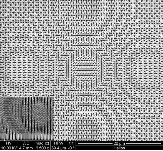
Rotation: the rotation of nanofin structures which creates a Pancharatnam–Berry phase for metalens applications The metalens pattern is written by electron beam lithography on a GaN epilayer. The pattern has a minimum feature size of 200nm and minimum distance of 100nm. Later a layer of Ni metal is deposited as the etching mask by lift-off process. Finally, a ICP/RIE etching process is used to fabricate the high aspect ratio nanofins. A combination of physical etching using Ar as well as chemical etching using Cl2 plasma improves the etching rate . The recipe is optimized to obtain maximum aspect ratio and perfect vertical side wall.
The sample is composed of GaN nanofins on a sapphire substrate. Firstly, the pattern is designed and written on the wafer by electron beam lithography. Then a layer of Ni is deposited on the wafer after which a lift-off process is carried out. Eventually, a layer of Ni hard mask is left on the wafer. While this is very thin, it is limited by the effectiveness of the lift-off process.
The most challenging process in this part is the etching of high aspect ratio nanofins. The width of each nanofin is around 200 nm and the height is ~1.5um, and the narrowest gap is a few tens of nm. We used the Oxford Instruments PlasmaLab System 100 to achieve this. The etching is in Ar plasma and gas mixture of Cl2/BCl3, which combines the physical etching of Ar plasma and the chemical etching of Cl2/BCl3. To get the highest etching selectivity and vertical sidewall, there are quite a few etching parameters to tune, such as the RF power, ICP power, Cl2/BCl3 ratio, and pressure.
Two main factors are at play here, on the one hand, we want more chemical etching to achieve higher selectivity because the metal mask is relatively thin. On the other hand, we want more physical etching to get the vertical sidewall. The actual recipe strikes a balance between these two processes. Eventually, by optimizing our recipe, we were able to reach a selectively of around 30 between Ni and GaN and a good sidewall quality.
Oxford Instruments systems have a user-friendly interface, which makes the recipe modification and sample loading very easy with minimal manual interventions required. Also, I was able to achieve good repeatability and uniformity over large scale sample surface thanks to the stability of Oxford Instruments systems. Overall my experience with Oxford Instruments is a pleasant one.

© Oxford Instruments 2026

