 Part of the Oxford Instruments Group
Expand
Collapse
Part of the Oxford Instruments Group
by: Peyman Yousefi, Chair for Laserphysics,
Friedrich-Alexander University of Erlangen-Nuremberg, Germany
Photonics-based laser accelerators are enticing candidates for future particle accelerators. They could reduce the size of current large radio-frequency accelerators by one to two orders of magnitude. This could essentially lead to compact high-energy electron sources for a variety of applications in medicine and high-energy physics. Our research centers on demonstrating the required steps towards this new kind of laser-powered accelerator.
To demonstrate such a concept, we use silicon as the substrate material and use a top-down approach to fabricate our desired structures. The fabrication process consists of two major steps, namely electron beam lithography as a high-resolution patterning technique and inductively coupled plasma reactive ion etching (ICP-RIE) as an anisotropic etching technique to transfer the written patterns into the substrate. We write the patterns on a negative tone resist with a reasonable etching durability.
After developing the resist, we then etch the silicon substrates by a PlasmaPro 100 RIE Oxford Instruments etcher, using SF6 and O2 as the etching components. A good control over the ratio of the two gases is essential to have a perfect anisotropic etching with a high selectivity. The etching starts by igniting a stable plasma in the chamber.
Once the plasma is formed, the radicals start to accelerate towards the substrate. Fluorine and oxygen radicals interact chemically with the silicon substrate forming a passive layer of SiOxFy. This prevents lateral etching throughout the process. However an optimized ratio of SF6 and O2 is essential to keep the passivation rate and the etching rate in balance. We have developed an etching process with an etch rate of 32 nm/s for a perfect anisotropic etching and smooth sidewalls. Our silicon structures are 3 μm tall with an aspect ratio of 20, making them ideal to perform our experiments around photonics-based particle acceleration.
Figure 1 shows a two-stage silicon dual pillar accelerator equipped with Bragg reflectors, which is comprised of four solid walls left of the dual pillar photonics accelerator structure in the upper right. This device is capable of delivering accelerated electrons with attosecond pulse
durations. An aperture in front is etched for alignment purposes. This device structure together with the attosecond electron bunch generation represent a major breakthrough towards an on-chip laser-driven particle accelerator[1, 2]. See achip.fau.de for more details.
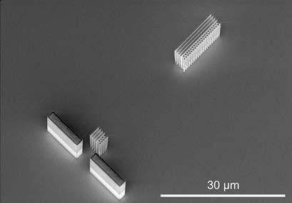
Figure 1. A two-stage silicon accelerator device fabricated by electron beam lithography and inductively coupled plasma reactive ion etching (ICP-RIE).

© Oxford Instruments 2026

